


ADSP-21020
REV. C
–26–
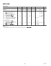
ENVIRONMENTAL CONDITIONS
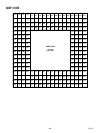
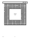
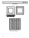
The ADSP-21020 is available in a Ceramic Pin Grid Array
(CPGA). The package uses a cavity-down configuration which
gives it favorable thermal characteristics. The top surface of the
package contains a raised copper slug from which much of the
die heat is dissipated. The slug provides a surface for mounting
a heat sink (if required).
The commercial grade (K grade) ADSP-21020 is specified for
operation at T
AMB
of 0°C to +70°C. Maximum T
CASE
(case
temperature) can be calculated from the following equation:
T
CASE
= T
AMB
+ PD ×θ
CA
()
where PD is power dissipation and θ
CA
is the case-to-ambient
thermal resistance. The value of PD depends on your
application; the method for calculating PD is shown under
“Power Dissipation” below. θ
CA
varies with airflow and with the
presence or absence of a heat sink. Table IX shows a range of
θ
CA
values.
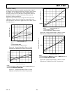
Table IX. Maximum θ
CA
for Various Airflow Values
Airflow (Linear ft./min.) 0 100 200 300
CPGA with No Heat Sink 12.8°C/W 9.2°C/W 6.6°C/W 5.5°C/W
NOTES
θ
JC
is approximately 1°C/W.
Maximum recommended T
J
is 130°C.
As per method 1012 MIL-STD-883. Ambient temperature: 25°C. Power:
3.5 W.
Power Dissipation
Total power dissipation has two components: one due to
internal circuitry and one due to the switching of external
output drivers. Internal power dissipation is dependent on the
instruction execution sequence and the data values involved.
Internal power dissipation is calculated in the following way:
P
INT
= I
DDIN
؋ V
DD
The external component of total power dissipation is caused by
the switching of output pins. Its magnitude depends on:
1) the number of output pins that switch during each cycle (O),
2) the maximum frequency at which they can switch (f),
3) their load capacitance (C), and
4) their voltage swing (V
DD
).
It is calculated by:
P
EXT
= O ؋ C ؋ V
DD
2
؋ f
The load capacitance should include the processor’s package
capacitance (C
IN
). The switching frequency includes driving the
load high and then back low. Address and data pins can drive
high and low at a maximum rate of 1/(2t
CK
). The write strobes
can switch every cycle at a frequency of 1/t
CK
. Select pins switch
at 1/(2t
CK
), but 2 DM and 2 PM selects can switch on each
cycle. If only one bank is accessed, no select line will switch.
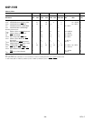
Example:
Estimate P
EXT
with the following assumptions:
•
A system with one RAM bank each of PM (48 bits) and DM
(32 bits).
•
32K ؋ 8 RAM chips are used, each with a load of 10 pF.
•
Single-precision mode is enabled so that only 32 data pins can
switch at once.
•
PM and DM writes occur every other cycle, with 50% of the
pins switching.
•
The instruction cycle rate is 20 MHz (t
CK
= 50 ns) and
V
DD
= 5.0 V.
The P
EXT
equation is calculated for each class of pins that can
drive:
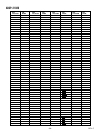
Pin # %
Type Pins Switch ؋ C ؋ f ؋ V
DD
2
P
EXT
PMA 15 50 68 pF 5 MHz 25 V 0.064 W
PMS 2 0 68 pF 5 MHz 25 V 0.000 W
PMWR 1 — 68 pF 10 MHz 25 V 0.017 W
PMD 32 50 18 pF 5 MHz 25 V 0.036 W
DMA 15 50 48 pF 5 MHz 25 V 0.045 W
DMS 2 0 48 pF 5 MHz 25 V 0.000 W
DMWR 1 — 48 pF 10 MHz 25 V 0.012 W
DMD 32 50 18 pF 5 MHz 25 V 0.036 W
P
EXT
=0.210 W
A typical power consumption can now be calculated for this
situation by adding a typical internal power dissipation:
P
TOTAL
= P
EXT
+ (5 V ؋ I
DDIN
(typ)) = 0.210 + 1.15
= 1.36 W
Note that the conditions causing a worst case P
EXT
are different
from those causing a worst case P
INT
. Maximum P
INT
cannot
occur while 100% of the output pins are switching from all ones
to all zeros. Also note that it is not common for a program to
have 100% or even 50% of the outputs switching simultaneously.
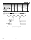
Power and Ground Guidelines
To achieve its fast cycle time, including instruction fetch, data
access, and execution, the ADSP-21020 is designed with high
speed drivers on all output pins. Large peak currents may pass
through a circuit board’s ground and power lines, especially
when many output drivers are simultaneously charging or
discharging their load capacitances. These transient currents can
cause disturbances on the power and ground lines. To minimize
these effects, the ADSP-21020 provides separate supply pins for
its internal logic (IGND and IVDD) and for its external drivers
(EGND and EVDD).
To reduce system noise at low temperatures when transistors
switch fastest, the ADSP-21020 employs compensated output
drivers. These drivers equalize slew rate over temperature
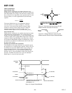
extremes and process variations. A 1.8 kΩ resistor placed
between the RCOMP pin and EVDD (+5 V) provides a
reference for the compensated drivers. Use of a capacitor
(approximately 100 pF), placed in parallel with the 1.8 kΩ
resistor, is recommended.