


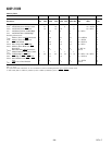

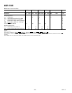
ADSP-21020
REV. C
–24–
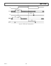
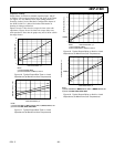
TEST CONDITIONS
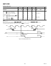
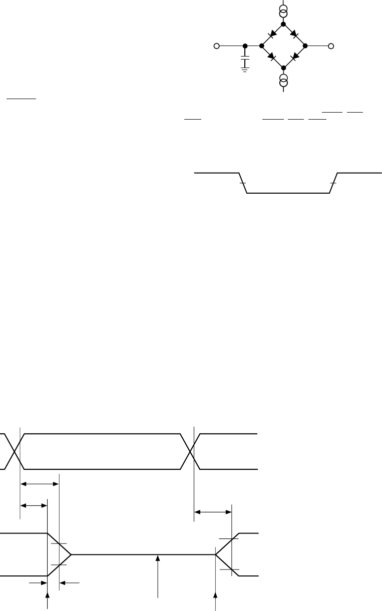
Output Disable Time
Output pins are considered to be disabled when they stop
driving, go into a high-impedance state, and start to decay from
their output high or low voltage. The time for the voltage on the
bus to decay by ∆V is dependent on the capacitive load, C
L
, and
the load current, I
L
. It can be approximated by the following
equation:
t
DECAY
=
C
L
∆V
I
L
The output disable time (t
DIS
) is the difference between
t
MEASURED
and t
DECAY
as shown in Figure 13. The time
t
MEASURED
) is the interval from when the reference signal
switches to when the output voltage decays ∆V from the
measured output high or output low voltage. t
DECAY
is
calculated with ∆V equal to 0.5 V, and test loads C
L
and I
L
.
Output Enable Time
Output pins are considered to be enabled when they have made
a transition from a high-impedance state to when they start
driving. The output enable time (t
ENA
) is the interval from when
a reference signal reaches a high or low voltage level to when the
output has reached a specified high or low trip point, as shown
in the Output Enable/Disable diagram. If multiple pins (such as
the data bus) are enabled, the measurement value is that of the
first pin to start driving.
Example System Hold Time Calculation
To determine the data output hold time in a particular system,
first calculate t
DECAY
using the above equation. Choose ∆V to be
the difference between the ADSP-21020’s output voltage and
the input threshold for the device requiring the hold time. A
typical ∆V will be 0.4 V. C
L
is the total bus capacitance (per
data line), and I
L
is the total leakage or three-state current (per
data line). The hold time will be t
DECAY
plus the minimum
disable time (i.e. t
HDWD
for the write cycle).
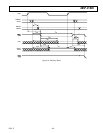
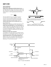
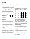
TO
OUTPUT
PIN
50pF
*
+1.5V
*
AC TIMING SPECIFICATIONS ARE CALCULATED FOR 100pF
DERATING ON THE FOLLOWING PINS: PMA23–0, PMS1–0, PMRD,
PMWR, PMPAGE, DMA31–0, DMS3–0, DMRD, DMWR, DMPAGE
I
OH
I
OL
Figure 14. Equivalent Device Loading For AC
Measurements (Includes All Fixtures)
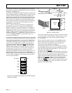
INPUT OR
OUTPUT
1.5V
1.5V
Figure 15. Voltage Reference Levels For AC
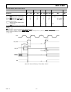
Measurements (Except Output Enable/Disable)
t
ENA
2.0V
1.0V
–∆V
+∆V
t
DIS
REFERENCE
SIGNAL
OUTPUT
t
DECAY
V
OH (MEASURED)
V
OL (MEASURED)
t
MEASURED
OUTPUT STOPS DRIVING
OUTPUT STARTS DRIVING
HIGH-IMPEDANCE STATE. TEST CONDITIONS
CAUSE THIS VOLTAGE LEVEL TO BE
APPROXIMATELY 1.5 V.
V
OH (MEASURED)
V
OL (MEASURED)
V
OH (MEASURED)
V
OL (MEASURED)
Figure 13. Output Enable/Disable