


ADSST-SALEM-3T
Rev. 0 | Page 5 of 24
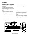
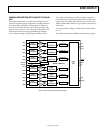
Efficient data transfer is achieved with the use of five internal
buses:
• Program Memory Address (PMA) Bus Program Memory
Data (PMD) Bus
• Data Memory Address (DMA) Bus
• Data Memory Data (DMD) Bus
• Result (R) Bus
The byte memory and I/O memory space interface supports
slow memories and I/O memory-mapped peripherals with pro-
grammable wait state generation. External devices can gain
control of external buses with bus request/grant signals (
BR
,
BGH
, and
BG0
). One execution mode (go mode) enables the
ADSST-218x to continue running from on-chip memory. Nor-
mal execution mode requires the processor to halt while buses
are granted.
The ADSST-218x can respond to 11 interrupts. There are up to
six external interrupts (one edge sensitive, two level sensitive,
and three configurable) and seven internal interrupts generated
by the timer, the serial ports (SPORTs), the byte DMA port, and
the power-down circuitry. There is also a master
RESET
signal.
The two serial ports provide a complete synchronous serial
interface with optional companding in hardware and a wide
variety of framed or frameless data transmit and receive modes
of operation.
Serial Ports
The ADSST-218x incorporates two complete synchronous serial
ports (SPORT0 and SPORT1) for serial communications and
multiprocessor communication.
Package Description
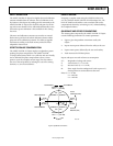
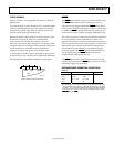
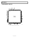
The ADSST-218x is available in a 100-lead low profile quad flat
package (LQFP, refer to Figure 5).