


ADSST-SALEM-3T
Rev. 0 | Page 8 of 24
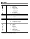
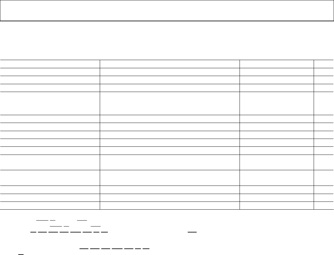
ADSST-218X ELECTRICAL CHARACTERISTICS
Table 4.
Parameter Test Conditions Min Typ Max Unit
V
IH
High Level Input Voltage
1, 2
@ V
DDINT
= Max 1.5 V
V
IH
High Level CLKIN Voltage @ V
DDINT
= Max 2.0 V
V
IL
Low Level Input Voltage
1, 3
@ V
DDINT
= Min 0.7 V
V
OH
High Level Output Voltage
1, 4, 5
@ V
DDEXT
= Min, I
OH
= –0.5 mA 2.0 V
@ V
DDEXT
= 3.0 V, I
OH
= –0.5 mA 2.4 V
@ V
DDEXT
= Min, I
OH
= –100 µA
6
V
DDEXT
– 0.3 V
V
OL
Low Level Output Voltage
1, 4, 5
@ V
DDEXT
= Min, I
OL
= 2 mA 0.4 V
I
IH
High Level Input Current
3
@ V
DDINT
= Max, V
IN
= 3.6 V 10 µA
I
IL
Low Level Input Current
3
@ V
DDINT
= Max, V
IN
= 0 V 10 µA
I
OZH
Three-State Leakage Current
7
@ V
DDEXT
= Max, V
IN
= 3.6 V
8
10 µA
I
OZL
Three-State Leakage Current
7
@ V
DDEXT
= Max, V
IN
= 0 V
8
10 µA
I
DD
Supply Current (Idle)
9
@ V
DDINT
= 2.5 V, t
CK
= 15 ns 9 mA
@ V
DDINT
= 2.5 V, t
CK
= 13.3 ns 10 mA
I
DD
Supply Current (Dynamic)
10
@ V
DDINT
= 2.5 V, t
CK
= 13.3 ns
11
, T
AMB
= +25°C 35 mA
@ V
DDINT
= 2.5 V, t
CK
= 15 ns
11
, T
AMB
= +25°C 38 mA
I
DD
Supply Current (Power-Down)
12
@ V
DDINT
= 2.5 V, T
AMB
= +25°C in Lowest Power Mode 100 mA
C
I
Input Pin Capacitance
3, 6
@ V
IN
= 2.5 V, f
IN
= 1.0 MHz, T
AMB
= +25°C 8 pF
C
O
Output Pin Capacitance
6, 7, 12, 13
@ V
IN
= 2.5 V, f
IN
= 1.0 MHz, T
AMB
= +25°C 8 pF
1
Bidirectional pins: D0–D23, RFS0, RFS1, SCLK0, SCLK1, TFS0, TFS1, A1–A13, PF0–PF7.
2
Input only pins:
RESET
,
BR
, DR0, DR1,
PWD
.
3
Input only pins: CLKIN,
RESET
,
BR
, DR0, DR1,
PWD
.
4
Output pins:
BG
,
PMS
,
DMS
,
BMS
,
IOMS
,
CMS
,
RD
,
WR
, PWDACK, A0, DT0, DT1, CLKOUT, FL2–0,
BGH
.
5
Although specified for TTL outputs, all ADSP-2186 outputs are CMOS compatible and will drive to V
DDEXT
and GND, assuming no dc loads.
6
Guaranteed but not tested.
7
Three-statable pins: A0–A13, D0–D23,
PMS
,
DMS
,
BMS
,
IOMS
,
CMS
,
RD
,
WR
, DT0, DT1, SCLK0, SCLK1, TFS0, TFS1, RFS0, RFS1, PF0–PF7.
8
0 V on
BR
.
9
Idle refers to ADSST-218x state of operation during execution of IDLE instruction. Deasserted pins are driven to either V
DD
or GND.
10
I
DD
measurement taken with all instructions executing from internal memory. 50% of the instructions are multifunction (Types 1, 4, 5, 12, 13, 14), 30% are Type 2 and
Type 6, and 20% are idle instructions.
11
V
IN
= 0 V and 3 V. For typical figures for supply currents, refer to the Power Dissipation section.
12
Applies to LQFP package type.
13
Output pin capacitance is the capacitive load for any three-stated output pin.