


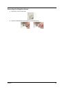

Chapter 4 63
POST Check Points
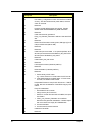
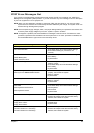
When POST executes a task, it uses a series of preset numbers called check point to be latched at port 80h,
indicating the stages it is currently running. This latch can be read and shown on a debug board.
The following table describes the Acer common tasks carried out by POST. A unique check point number
represents each task.
Checkpoint Description
CFh Test CMOS R/W functionality
C0h Early chipset initialization:
• Disable shadow RAM
• Disable L2 Cache (socket 7 or below)
• Program basic chipset registers
C1h Detect memory
• Auto-detection of DRAM size, type and ECC.
• Auto-detection of L2 cache (socket 7 or below)
C3h Expand compressed BIOS code to DRAM
C5h Call chipset hook to copy BIOS back to E000 & F000
shadow RAM
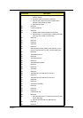
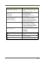
0h1 Expand the Xgroup codes locating in physical address
1000:0
02h Reserved
03h Initial Superio_Early_Init switch
04h Reserved
05h 1. Blank out screen
2. Clear CMOS error flag
06h Reserved
07h 1. Clear 8042 interface
2. Initialize 8042 self-test
08h 1. Test special keyboard controller for Winbond 977 series
Super I/O chips
2. Enable keyboard interface
09h Reserved
0Ah 1. Disable PS/2 mouse interface (optional)
2. Auto detect ports for keyboard & mouse followed by a
port & interface swap (optional)
3. Reset keyboard for Winbond 977 series Super I/O
chips
0Bh Reserved
0Ch Reserved
0Dh Reserved
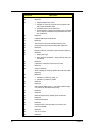
0Eh Test F000h segment shadow to see whether it is R/W-able
or not. If test fails. keep beeping the speaker.
0Fh Reserved
10h Auto detect flash type to load appropriate flash R/W codes
into the run time area in F000 for ESCD & DMI support.