


2-18
Chapter 2: BIOS information
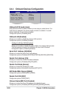
The following sub-items appear only when the item Configure DRAM Timing
by SPD is set to Disabled.
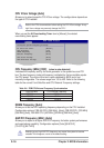
Configure DRAM Timing by SPD [Enabled]
When this item is enabled, the DRAM timing parameters are set according to the
DRAM SPD (Serial Presence Detect). When disabled, you can manually set the
DRAM timing parameters through the DRAM sub-items.
Configuration options: [Disabled] [Enabled]
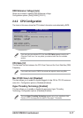
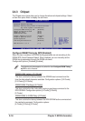
2.4.3 Chipset
The Chipset menu items allow you to change the advanced chipset settings. Select
an item then press Enter to display the sub-menu.
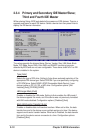
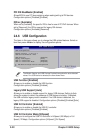
Advanced Chipset Settings
Warning: Setting wrong values in below sections
may cause system to malfunction.
Configure DRAM Timing by SPD [Enabled]
Memory Acceleration Mode [Auto]
DRAM Idle Timer [Auto]
DRAM Refresh Rate [Auto]
Graphic Adapter Priority [AGP/PCI]
Graphics Aperture Size [ 64MB]
Spread Spectrum [Enabled]
ICH Delayed Transaction [Enabled]
MPS Revision 1.1/1.4 [1.1]
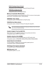
DRAM CAS# Latency [2.5 Clocks]
This item controls the latency between the SDRAM read command and the
time the data actually becomes available. Configuration options: [2.0 Clocks]
[2.5 Clocks] [3.0 Clocks]
DRAM RAS# Precharge [4 Clocks]
This item controls the idle clocks after issuing a precharge command to the
DDR SDRAM. Configuration options: [4 Clocks] [3 Clocks]
[2 Clocks]
DRAM RAS# to CAS# Delay [4 Clocks]
This item controls the latency between the DDR SDRAM active command and
the read/write command. Configuration options:
[4 Clocks] [3 Clocks] [2 Clocks]