


Using the STK502 Top Module
2-8 STK502 User Guide
2528A–AVR–11/02
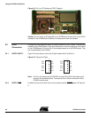
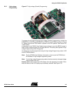
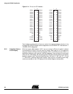
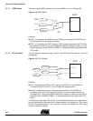
Figure 2-11. Pin out for LCD Headers
This hardware configuration will give a certain bit-mapping between the bits in the
ATmega169 LCDDRx Register and the segments on the STK502 LCD. See Section 4.1
“STK502 LCD Bit Mappings”
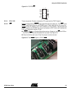
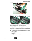
2.5.3 Using Both Colons
on the Display
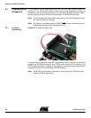
With the header J300 labelled “19 24” one can connect LCD-pin 24 (which is default
unconnected) to LCD-pin 19 by the use of a jumper. See Figure 2-12. The reason for
doing so is that the LCD-pin 24 has the segment “COL1” and LCD-pin 19 has “COL2”. In
applications where a clock, date etc. shall be displayed, it can be useful to control both
colons on the LCD-display. But connecting these LCD-pins will also lead to a connection
between segment (see Technical Specifications) “S5” and “3”, “S8” and “S7”, “8” and
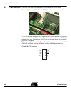
“7”, which will in practice make them useless. See Figure 2-13 showing which seg-
ments are available on the LCD-display with the default segment configuration.
SEG01
SEG03
SEG05
SEG07
SEG09
SEG11
SEG13
SEG15
SEG17
SEG19
SEG21
SEG23
SEG25
NC
NC
COM00
COM02
SEG02
SEG04
SEG06
SEG08
SEG10
SEG12
SEG14
SEG16
SEG18
SEG20
SEG22
SEG24
NC
NC
NC
COM01
COM03
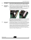
Seg. M169
1 2
LCD27
LCD29
LCD06
LCD26
LCD08
LCD23
LCD10
LCD21
LCD14
LCD11
LCD18
LCD15
LCD19
LCD24
LCD31
BP1
BP4
LCD2
8
LCD0
4
LCD2
5
LCD0
5
LCD2
2
LCD0
7
LCD2
0
LCD0
9
LCD1
2
LCD1
3
LCD1
6
LCD1
7
LCD0
3
LCD3
0
LCD3
2
BP2
BP3
LCD Pins
1 2