


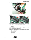
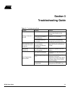

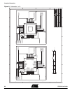

Technical Specifications
STK502 User Guide 4-3
2528A–AVR–11/02
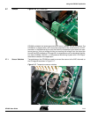
4.1 STK502 LCD Bit
Mappings
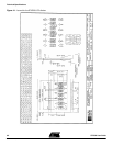
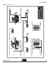
The LCD Data Registers (LCDDRx) in the ATmega169 are organized in groups accord-
ing to the use of Backplane Control Lines (also known as Common Lines). The LCD on
the STK502 uses all four Common Lines and all 25 segments, in total 4 x 25 = 100 seg-
ments. As can be seen in the LCD data sheet (Figure 4-1) describing the internal
connection of pins, Common Lines and segments, the alphanumeric digits are referred
to with a number according to where they are located on the LCD. Listed below is a
description of the STK502 bit mappings according to this.
4.1.1 Alphanumeric Digit
Number Two
The bit mappings for the alphanumeric digit number two are listed below.
4.1.2 Alphanumeric Digit
Number Three
The bit mappings for the alphanumeric digit number three are listed below.
4.1.3 Alphanumeric Digit
Number Four
The bit mappings for the alphanumeric digit number four are listed below.
4.1.4 Alphanumeric Digit
Number Five
The bit mappings for the alphanumeric digit number five are listed below.
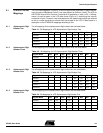
Table 4-1. Bit Mappings for LCD Alphanumeric Digit Number Two
Register Name Bit7 Bit6 Bit5 Bit4 Bit3 Bit2 Bit1 Bit0
LCDDR0 2-K 1 S1 2-A
LCDDR5 2-J 2-F 2-H 2-B
LCDDR10 2-L 2-E 2-G 2-C
LCDDR15 2-M 2-P 2-N 2-D
Table 4-2. Bit Mappings for LCD Alphanumeric Digit Number Three
Register Name Bit7 Bit6 Bit5 Bit4 Bit3 Bit2 Bit1 Bit0
LCDDR0 3-K 2 S2 3-A
LCDDR5 3-J 3-F 3-H 3-B
LCDDR10 3-L 3-E 3-G 3-C
LCDDR15 3-M 3-P 3-N 3-D
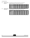
Table 4-3. Bit Mappings for LCD Alphanumeric Digit Number Four
Register Name Bit7 Bit6 Bit5 Bit4 Bit3 Bit2 Bit1 Bit0
LCDDR1 4-K S3 4 4-A
LCDDR6 4-J 4-F 4-H 4-B
LCDDR11 4-L 4-E 4-G 4-C
LCDDR16 4-M 4-P 4-N 4-D
Table 4-4. Bit Mappings for LCD Alphanumeric Digit Numer Five
Register Name Bit7 Bit6 Bit5 Bit4 Bit3 Bit2 Bit1 Bit0
LCDDR1 5-K S4 5 5-A
LCDDR6 5-J 5-F 5-H 5-B
LCDDR11 5-L 5-E 5-G 5-C
LCDDR16 5-M 5-P 5-N 5-D