


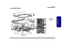
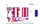
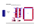
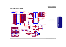
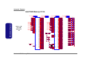
Schematic Diagrams
B-1
B.Schematic Diagrams
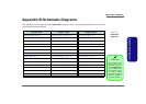
Appendix B:Schematic Diagrams
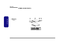
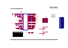
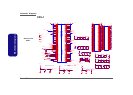
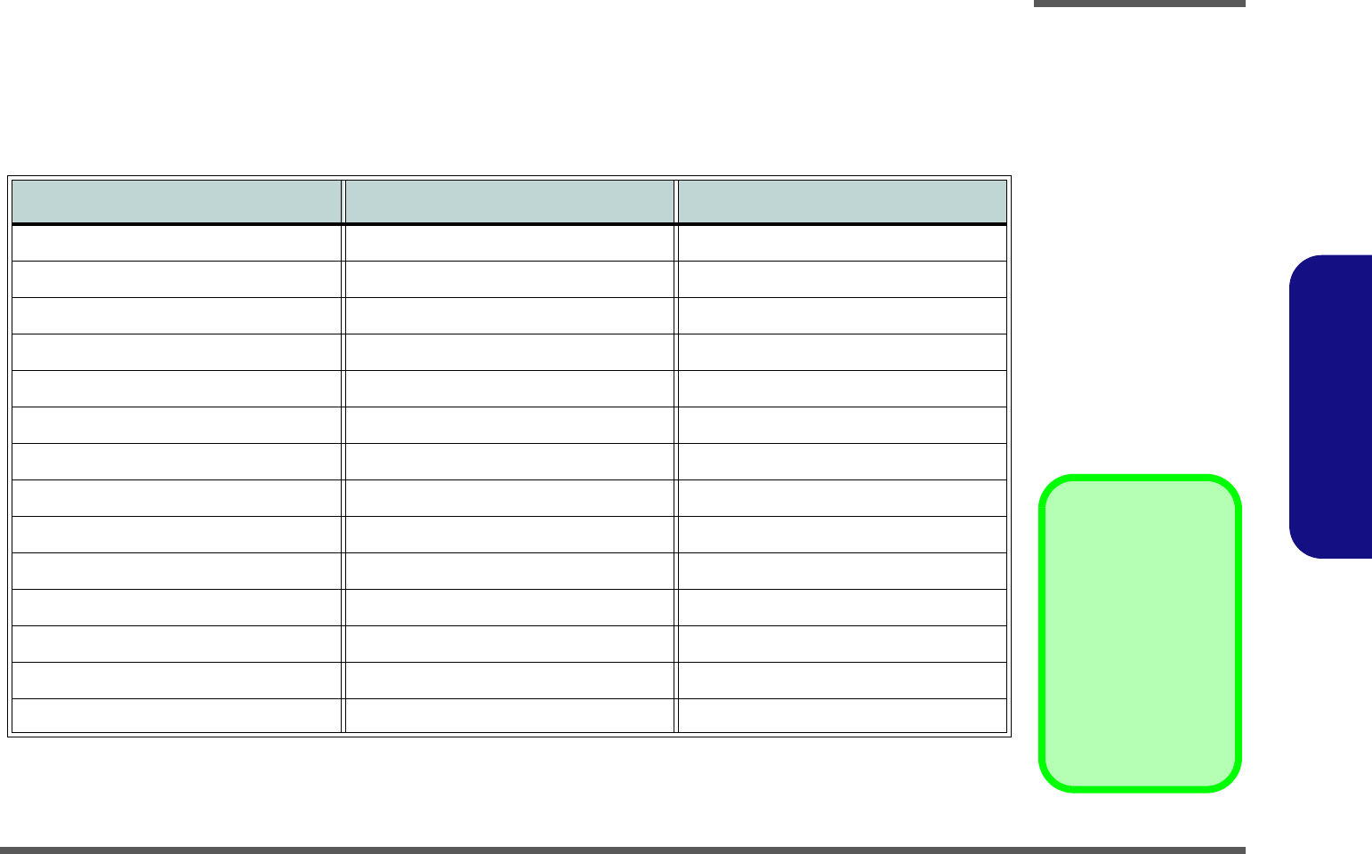
This appendix has circuit diagrams of the D900C/D901C notebook’s PCB’s. The following table indicates where to find
the appropriate schematic diagram.
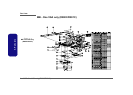
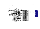
Diagram - Page Diagram - Page Diagram - Page
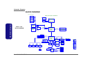
BLOCK DIAGRAM - Page B - 2 BR03 PCI-E & Straps 1/3 - Page B - 16 AC-In, Charger - Page B - 30
CLOCK GENERATOR - Page B - 3 BR03 PCI-E Interface 2/3 - Page B - 17 Power 1.2V/ 1.25V - Page B - 31
CPU-1 - Page B - 4 BR03 Power & GND 3/3 - Page B - 18 Power 1.5V/ 1.05V/ 2.5V - Page B - 32
CPU-2 - Page B - 5 DVI/ CRT - Page B - 19 Power 1.8V/ 0.9V/ 12V - Page B - 33
Intel P965 CPU Interface 1/4 - Page B - 6 Panel CON/ LED Indicator - Page B - 20 Power 3.3V/ 5V - Page B - 34
Intel P965 PCI- E I/F 2/4 - Page B - 7 1394/ Card Reader (TI PCI7402) - Page B - 21 VCore Power - Page B - 35
Intel P965 Memory I/F 3/4 - Page B - 8 GLAN RTL8111B - Page B - 22 Audio Board - Page B - 36
DDRII SODIMM - Page B - 9 Audio ALC888/ Amplifier - Page B - 23 Card Reader Board - Page B - 37
Intel P965 Power 4/4 - Page B - 10 KBC-H8/2111 - Page B - 24 Click Board - Page B - 38
ICH8 PCI, DMI, CPU, IRQ - Page B - 11 JM368 PCIE to PATA - Page B - 25 HotKey Board - Page B - 39
ICH8 LPC, ATA, USB, GPIO - Page B - 12 Mini Card & TV Out/ Video In - Page B - 26 Switch Board - Page B - 40
ICH8 Power - Page B - 13 Daughter Connection - Page B - 27 USB Board - Page B - 41
MXM PCI-E CON1 - Page B - 14 CCD/ BT/ FAN/ ROM - Page B - 28
MXM PCI-E CON2 - Page B - 15 Mini PCI/ MDC/ New Card - Page B - 29
Table B - 1
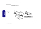
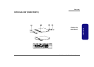
Schematic
Diagrams
Version Note
The schematic dia-
grams in this chapter
are based upon ver-
sion 6-7P-D90C7-006.
If your mainboard (or
other boards) are a lat-
er version, please
check with the Service
Center for updated di-
agrams (if required).