


PRELIMINARY
CY14B104K, CY14B104M
Document #: 001-07103 Rev. *K Page 2 of 31
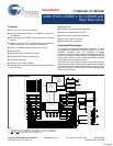
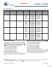
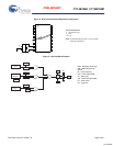
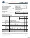
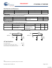
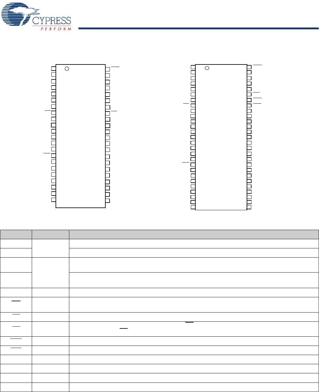
Pinouts
Figure 1. Pin Diagram - 44-PIn and 54-Pin TSOP II
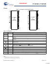
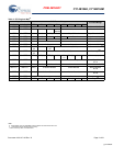
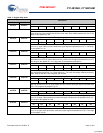
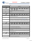
Table 1. Pin Definitions
Pin Name I/O Type Description
A
0
– A
18
Input Address Inputs Used to Select one of the 524,288 bytes of the nvSRAM for x8 Configuration.
A
0
– A
17
Address Inputs Used to Select one of the 262,144 words of the nvSRAM for x16 Configuration.
DQ
0
– DQ
7
Input/Output Bidirectional Data I/O Lines for x8 Configuration. Used as input or output lines depending on
operation.
DQ
0
– DQ
15
Bidirectional Data I/O Lines for x16 Configuration. Used as input or output lines depending on
operation.
NC No Connect No Connects. This pin is not connected to the die.
WE
Input Write Enable Input, Active LOW. When selected LOW, data on the I/O pins is written to the specific
address location.
CE
Input Chip Enable Input, Active LOW. When LOW, selects the chip. When HIGH, deselects the chip.
OE
Input Output Enable, Active LOW. The active LOW OE input enables the data output buffers during read
cycles. Deasserting OE
HIGH causes the I/O pins to tri-state.
BHE
Input Byte High Enable, Active LOW. Controls DQ
15
- DQ
8
.
BLE
Input Byte Low Enable, Active LOW. Controls DQ
7
- DQ
0
.
X
1
Output Crystal Connection. Drives crystal on start up.
X
2
Input Crystal Connection. For 32.768 KHz crystal.
V
RTCcap
Power Supply Capacitor Supplied Backup RTC Supply Voltage. Left unconnected if V
RTCbat
is used.
V
RTCbat
Power Supply Battery Supplied Backup RTC Supply Voltage. Left unconnected if V
RTCcap
is used.
NC
A
8
X2
X1
V
SS
DQ
6
DQ5
DQ4
V
CC
A
13
DQ
3
A
12
DQ
2
DQ
1
DQ
0
OE
A
9
CE
NC
A
0
A
1
A
2
A
3
A
4
A
5
A
6
A
11
A
7
A
14
A
15
A
16
NC
1
2
3
4
5
6
7
8
9
10
11
12
13
14
15
16
17
18
19
20
21
22
23
24
25
26
27
28
29
30
31
32
33
34
35
36
37
38
39
40
41
42
43
44
44 - TSOP II
Top View
(not to scale)
A
10
V
RTCbat
WE
DQ
7
HSB
INT
V
SS
V
CC
V
CAP
V
RTCcap
(x8)
DQ
7
DQ
6
DQ
5
DQ
4
V
CC
DQ
3
DQ
2
DQ
1
DQ
0
NC
A
0
A
1
A
2
A
3
A
4
A
5
A
6
A
7
V
CAP
WE
A
8
A
10
A
11
A
12
A
13
A
14
A
15
1
2
3
4
5
6
7
8
9
10
11
12
13
14
15
16
17
18
19
20
21
22
23
24
25
26
27
28
29
30
31
32
33
34
35
36
37
38
39
40
41
42
43
44
45
46
47
48
54 - TSOP II
Top View
(not to scale)
OE
CE
V
CC
INT
V
SS
NC
A
9
NC
NC
54
53
52
51
49
50
HSB
BHE
BLE
DQ
15
DQ
14
DQ
13
DQ
12
V
SS
DQ
11
DQ
10
DQ
9
DQ
8
(x16)
V
RTCcap
V
RTCbat
X2
X1
[4]
[4]
[5]
[5]
A
17
A
18
A
16
A
17
Notes
4. Address expansion for 8 Mbit. NC pin not connected to die.
5. Address expansion for 16 Mbit. NC pin not connected to die.
[+] Feedback