ADVANCE
CY14B108L, CY14B108N
Document Number: 001-45523 Rev. *A Page 11 of 20
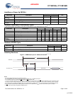
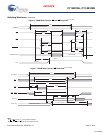
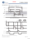
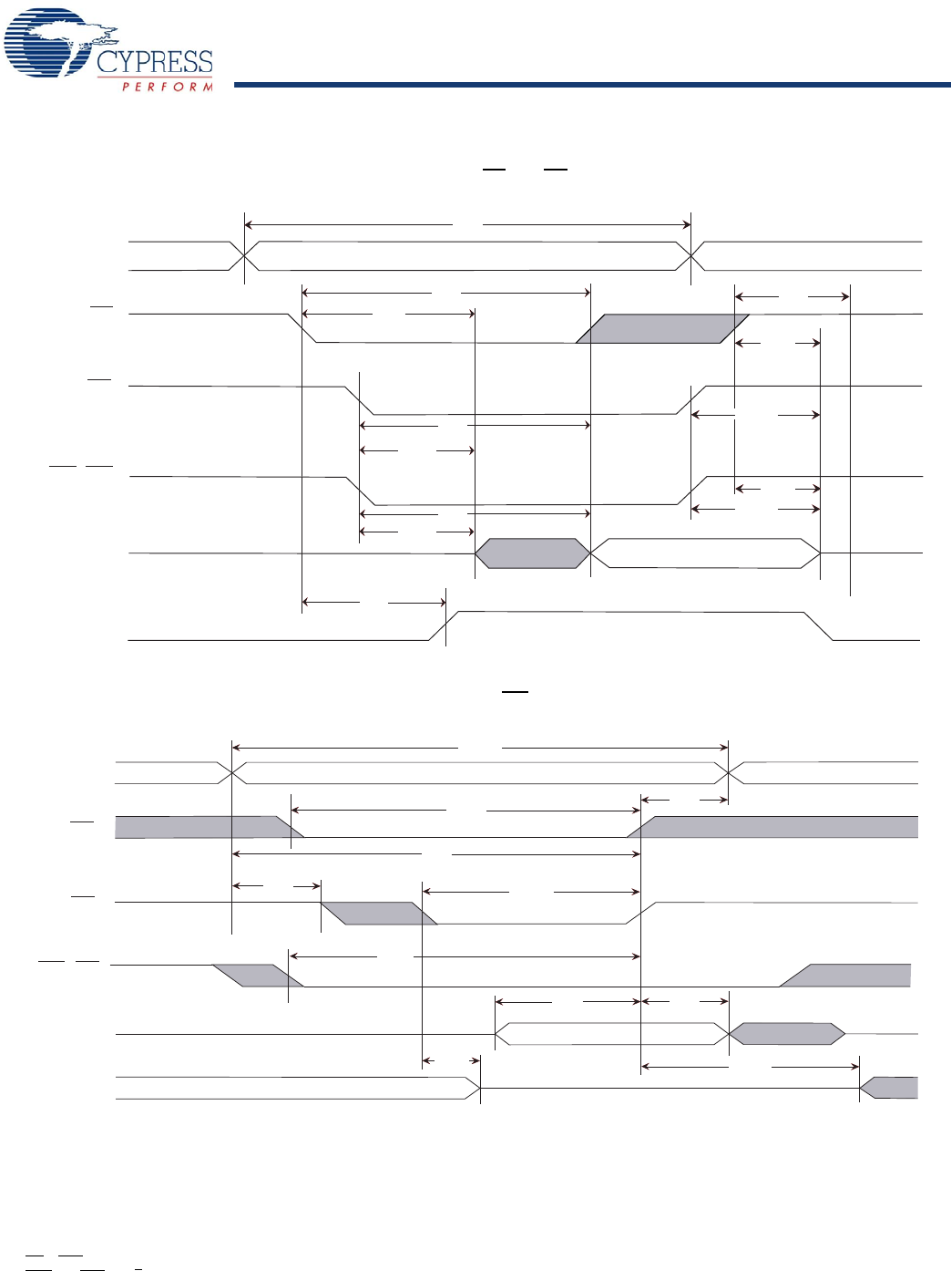
Figure 6. SRAM Read Cycle #2: CE
and OE Controlled
[10, 21, 23]
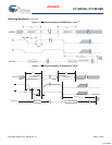
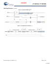
Figure 7. SRAM Write Cycle #1: WE Controlled
[13, 21, 22, 23]
Switching Waveforms (continued)
ADDRESS
t
RC
CE
t
ACE
t
LZCE
t
PD
t
HZCE
OE
t
DOE
t
LZOE
DATA VALID
ACTIVE
STANDBY
t
PU
DQ (DATA OUT)
ICC
t
LZBE
t
DBE
t
HZBE
HZOE
t
t
HZCE
BHE , BLE
t
WC
t
SCE
t
HA
t
AW
t
SA
t
PWE
t
SD
t
HD
t
HZWE
t
LZWE
ADDRESS
CE
WE
DATA IN
DATA OUT
DATA VALID
HIGH IMPEDANCE
PREVIOUS DATA
BHE , BLE
t
BW
Notes
22.CE
or WE must be >V
IH
during address transitions.
23.BHE
and BLE are applicable for x16 configuration only.
[+] Feedback


