


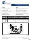
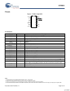
CY2291
Document #: 38-07189 Rev. *C Page 6 of 12
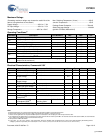
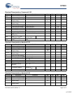
V
IH
HIGH-Level Input Voltage
[9]
Except crystal pins 2.0 V
V
IL
LOW-Level Input Voltage
[9]
Except crystal pins 0.8 V
I
IH
Input HIGH Current V
IN
= V
DD
–0.5V < 1 10 μA
I
IL
Input LOW Current V
IN
= +0.5V < 1 10 μA
I
OZ
Output Leakage Current Three-state outputs 250 μA
I
DD
V
DD
Supply Current
[10]
Industrial
V
DD
= V
DD
max., 3.3V operation 50 70 mA
I
DDS
V
DD
Power Supply Current
in Shutdown Mode
[10]
Shutdown active,
excluding V
BATT
CY2291I/CY2291FI 10 100 μA
I
BATT
V
BATT
Power Supply Current V
BATT
= 3.0V 5 15 μA
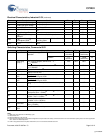
Switching Characteristics, Commercial 5.0V
Parameter Name Description Min. Typ. Max. Unit
t
1
Output Period Clock output range, 5V
operation
CY2291 10
(100 MHz)
13000
(76.923 kHz)
ns
CY2291F 11.1
(90 MHz)
13000
(76.923 kHz)
ns
Output Duty
Cycle
[11]
Duty cycle for outputs, defined as t
2
÷ t
1
[12]
f
OUT
> 66 MHZ
40% 50% 60%
Duty cycle for outputs, defined as t
2
÷ t
1
[12]
f
OUT
< 66 MHZ
45% 50% 55%
t
3
Rise Time
Output clock rise time
[13]
35ns
t
4
Fall Time
Output clock fall time
[13]
2.5 4 ns
t
5
Output Disable
Time
Time for output to enter three-state mode after
SHUTDOWN
/OE goes LOW
10 15 ns
t
6
Output Enable
Time
Time for output to leave three-state mode after
SHUTDOWN
/OE goes HIGH
10 15 ns
t
7
Skew
Skew delay between any identical or related outputs
[3,
12, 15]
< 0.25 0.5 ns
t
8
CPUCLK Slew Frequency transition rate 1.0 20.0 MHz/m
s
t
9A
Clock Jitter
[14]
Peak-to-peak period jitter (t
9A
Max. – t
9A
min.),% of
clock period (f
OUT
< 4 MHz)
< 0.5 1 %
t
9B
Clock Jitter
[14]
Peak-to-peak period jitter (t
9B
Max. – t
9B
min.)
(4 MHz <
f
OUT
< 16 MHz)
< 0.7 1 ns
t
9C
Clock Jitter
[14]
Peak-to-peak period jitter
(16 MHz < f
OUT
<
50 MHz)
< 400 500 ps
t
9D
Clock Jitter
[14]
Peak-to-peak period jitter
(f
OUT
> 50 MHz)
< 250 350 ps
t
10A
Lock Time for
CPLL
Lock Time from Power Up < 25 50 ms
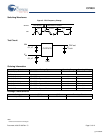
Electrical Characteristics, Industrial 3.3V (continued)
Parameter Description Conditions Min. Typ. Max. Unit
Notes
11.XBUF duty cycle depends on XTALIN duty cycle.
12.Measured at 1.4V.
13.Measured between 0.4V and 2.4V.
14.Jitter varies with configuration. All standard configurations sample tested at the factory conform to this limit. For more information on jitter, please refer to the application
note: “Jitter in PLL-Based Systems.”
15.CLKF is not guaranteed to be in phase with CLKA-D, even if it is referenced off the same PLL.
[+] Feedback