


CY24272
Document Number: 001-42414 Rev. ** Page 3 of 13
PLL Multiplier
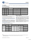
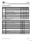
Table 3 shows the frequency multipliers in the PLL, selectable by programming the SMBus registers MULT0, MULT1, and MULT2.
Default multiplier at power up is 4.
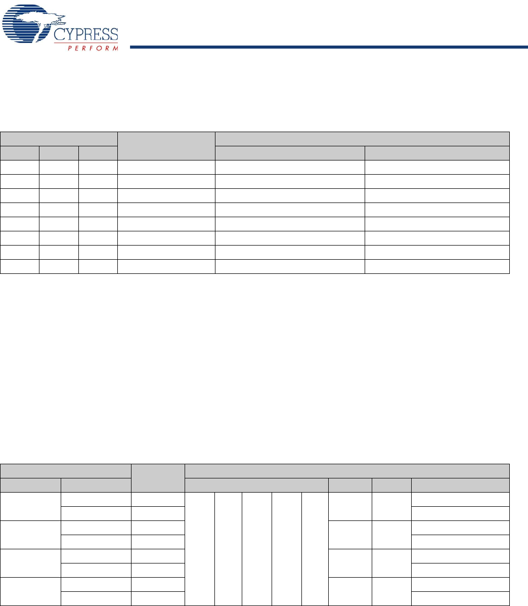
Table 3. PLL Multiplier Selection
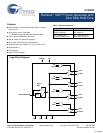
Input Clock Signal
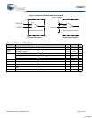
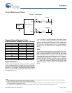
The XCG receives either a differential (REFCLK/REFCLKB) or a
single-ended reference clocking input (REFCLK).
When the reference input clock is from a different clock source,
it must meet the voltage levels and timing requirements listed in
DC Operating Conditions on page 7 and AC Operating Condi-
tions on page 8.
For a single-ended clock input, an external voltage divider and a
supply voltage, as shown in Figure 2 on page 6, provide a
reference voltage V
TH
at the REFCLKB pin. This determines the
proper trip point of REFCLK. For the range of V
TH
specified in
DC Operating Conditions on page 7, the outputs also meet the
DC and AC Operating Conditions tables.
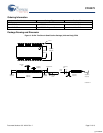
Modes of Operation
The modes of operation are determined by the logic signals
applied to the EN and /BYPASS pins and the values in the five
SMBus Registers: RegTest, RegA, RegB, RegC, and RegD.
Table 5 on page 4 shows selection from one to all four of the
outputs, the Outputs Disabled Mode (EN = low), and Bypass
Mode (EN = high, /BYPASS = low). There is an option reserved
for vendor test. Disabled outputs are set to High Z.
At power up, the SMBus registers default to the last entry in Table
6 on page 5. The value at RegTest is 0. The values at RegA,
RegB, RegC, and RegD are all ‘1’. Thus, all outputs are
controlled by the logic applied to EN and /BYPASS.
Notes
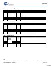
1. Output frequencies shown in Table 3 are based on nominal input frequencies of 100 MHz and 133.3 MHz. The PLL multipliers are applicable to spread spectrum
modulated input clock with maximum and minimum input cycle time. The REFSEL bit in SMBus 81h is set correctly as shown.
2. Default PLL multiplier at power up.
Register
Frequency Multiplier
Output Frequency (MHz)
MULT2 MULT1 MULT0 REFCLK = 100 MHz
[1]
, REFSEL = 0 REFCLK = 133 MHz
[1]
, REFSEL = 1
0 0 0 3 300 400
001 4 400
[2]
–
0 1 0 5 500 667
0 1 1 6 600 –
1 0 0 Reserved – –
1 0 1 9/2 450 600
1 1 0 Reserved – –
1 1 1 15/4 375 500
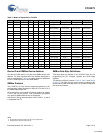
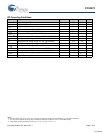
Table 4. SMBus Device Addresses for CY24272
XCG
Hex
Address
8-bit SMBus Device Address Including Operation
Device Operation Five Most Significant Bits ID1 ID0 WR# / RD
0
Write D8
11011
00
0
Read D9 1
1
Write DA
01
0
Read DB 1
2
Write DC
10
0
Read DD 1
3
Write DE
11
0
Read DF 1
[+] Feedback