


CY24272
Document Number: 001-42414 Rev. ** Page 6 of 13
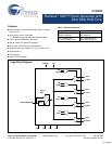
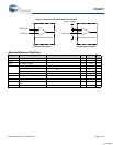
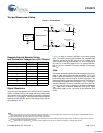
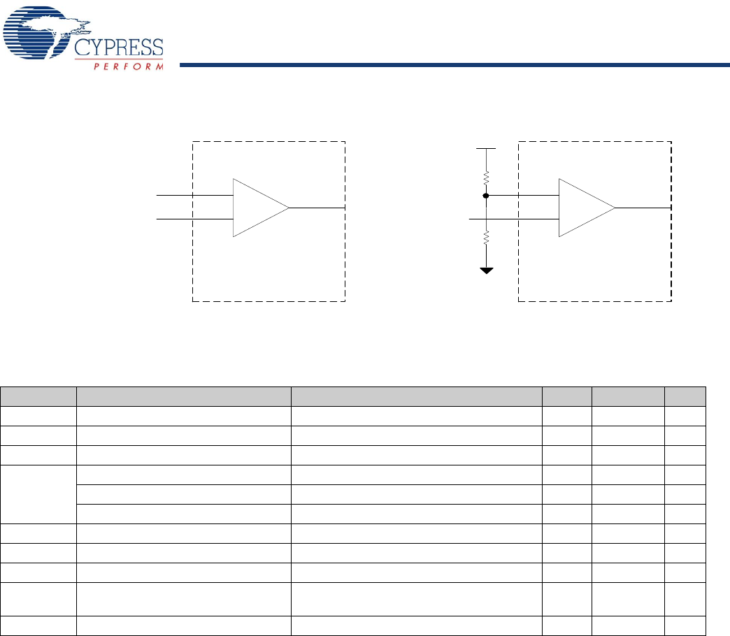
Figure 2. Differential and Single-Ended Clock Inputs
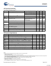
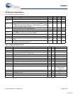
Absolute Maximum Conditions
Parameter Description Condition Min Max Unit
V
DD
Clock Buffer Supply Voltage –0.5 4.6 V
V
DDC
Core Supply Voltage –0.5 4.6 V
V
DDP
PLL Supply Voltage –0.5 4.6 V
V
IN
Input Voltage (SCL and SDA) Relative to V
SS
–0.5 4.6 V
Input Voltage (REFCLK/REFCLKB
) Relative to V
SS
–0.5 V
DD
+ 1.0 V
Input Voltage Relative to V
SS
–0.5 V
DD
+ 0.5 V
T
S
Temperature, Storage Non-functional –65 150 °C
T
A
Temperature, Operating Ambient Functional 0 70 °C
T
J
Temperature, Junction Functional – 150 °C
Ø
JA
Junction to Ambient thermal resis-
tance
Zero air flow – 100 °C/W
ESD
HBM
ESD Protection (Human Body Model) MIL-STD-883, Method 3015 2000 – V
REFCLKB
REFCLK
Input
XDR Clock Generator
Input
XDR Clock Generator
REFCLK
Supply Voltage
V
TH
Differential Input Single-ended Input
[+] Feedback