CY25818/19
Document #: 38-07362 Rev. *B Page 2 of 7
.
Overview
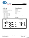
The Cypress CY25818/19 products are Spread Spectrum
Clock Generator (SSCG) ICs used for the purpose of reducing
EMI found in today’s high-speed digital electronic systems.
The devices use a Cypress proprietary phase-locked loop
(PLL) and Spread Spectrum Clock (SSC) technology to
synthesize and modulate the frequency of the input clock. By
frequency modulating the clock, the measured EMI at the
fundamental and harmonic frequencies is greatly reduced.
This reduction in radiated energy can significantly reduce the
cost of complying with regulatory agency requirements and
improve time to market without degrading system perfor-
mance.
The input frequency range is 8–16 MHz for the CY25818 and
16–32 MHz for the CY25819. Both products accept external
clock, crystal, or ceramic resonator inputs.
The CY25818/19 provide separate modulated (SSCLK) and
unmodulated reference (REFCLK) clock outputs which are the
same frequency as the input clock frequency. Down spread
frequency modulation can be selected by the user, based on
three discrete values of Spread%. A separate power down
function is also provided.
The CY25818/19 products are available in an 8-pin SOIC
(150-mil) package with a commercial operating temperature
range of 0–70°C. Contact Cypress for availability of –40 to
+85°C industrial temperature range operation or TSSOP
package versions. Refer to the CY25568, CY25811,
CY25812, and CY25814 products for other functions such as
clock multiplication of 1×, 2×, or 4× to generate a wide range
of Spread Spectrum output clocks from 4 to 128 MHz.
Input Frequency Range and Selection
CY25818/19 input frequency range is 8–32 MHz. This range
is divided into two segments, as given in Table 1.
Spread% Selection
CY25818/19 SSCG products provide Down-Spread frequency
modulation. The amount of Spread% is selected by using
3-Level S0 digital input. Spread% values are given in Table 2.
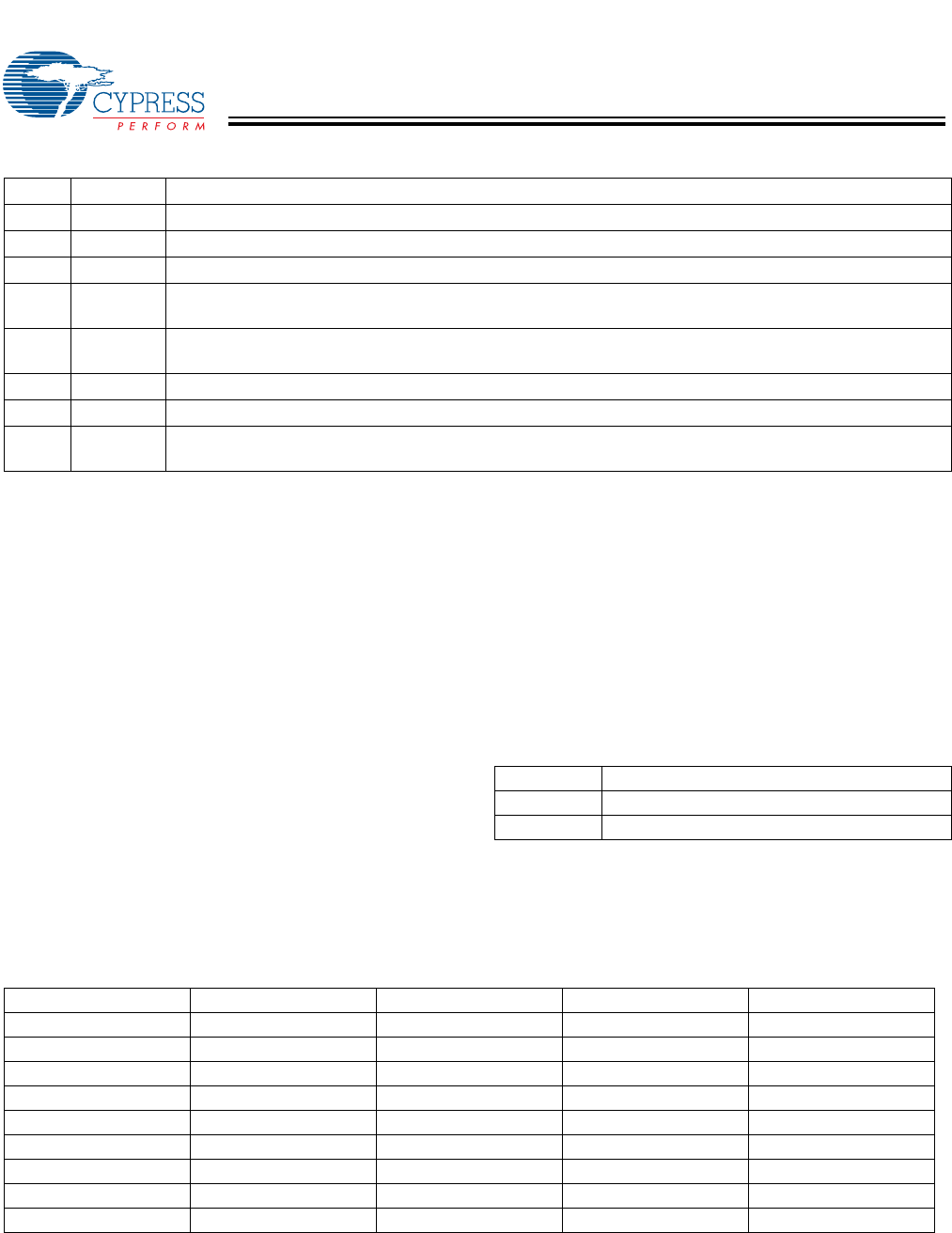
Pin Description
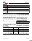
Pin Name Description
1 XIN/CLK Clock, Crystal, or Ceramic Resonator Input Pin.
2 Vss Power Supply Ground.
3 S0 Digital Spread% Control Pin. 3-Level input (H-M-L). Default = M.
4 SSCLK
Modulated Spread Spectrum Output Clock. The output frequency is referenced to input frequency. Refer
to Table 2 for the amount of modulation (Spread%).
5REFCLK
Unmodulated Reference Clock Output. The unmodulated output frequency is the same as the input
frequency.
6 PD# Power-Down Control Pin. Default = H (Vdd).
7 Vdd Positive Power Supply.
8XOUT
Clock, Crystal, or Ceramic Resonator Output Pin. Leave this pin unconnected if an external clock is used
at X
IN
pin.
Table 1. Input and Output Frequency Selection
Product Input/Output Frequency Range
CY25818 8–16 MHz
CY25819 16–32 MHz
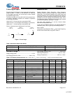
Table 2. Spread% Selection
XIN (MHz) Product S0 = 1 S0 = 0 S0 = M
Down (%) Down (%) Down (%)
8–10 CY25818 –3.0 –2.2 –0.7
10–12 CY25818 –2.7 –1.9 –0.6
12–14 CY25818 –2.5 –1.8 –0.6
14–16 CY25818 –2.3 –1.7 –0.5
16–20 CY25819 –3.0 –2.2 –0.7
20–24 CY25819 –2.7 –1.9 –0.6
24–28 CY25819 –2.5 –1.8 –0.6
28–32 CY25819 –2.3 –1.7 –0.5
[+] Feedback


