CY25818/19
Document #: 38-07362 Rev. *B Page 3 of 7
3-Level Digital Inputs
S0 digital input is designed to sense three logic levels desig-
nated as HIGH “1,” LOW “0,” and MIDDLE “M.” With this
3-Level digital input logic, the 3-Level logic is able to detect
three different logic levels.
The S0 pin includes an on-chip 20K (10K/10K) resistor divider.
No external application resistors are needed to implement
3-Level logic, as follows.
Logic Level “0”: 3-Level logic pin connected to GND.
Logic Level “M”: 3-Level logic pin left floating (no connection.)
Logic Level “1”: 3-Level logic pin connected to Vdd.
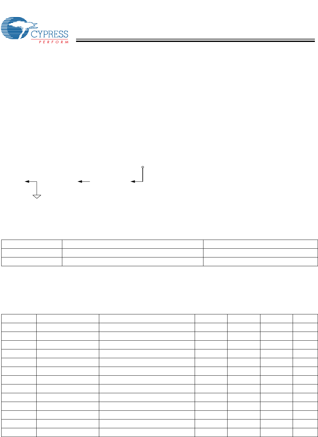
Figure 1 illustrates how to implement 3-Level Logic.
Modulation Rate
Spread Spectrum Clock Generators utilize frequency
modulation (FM) to distribute energy over a specific band of
frequencies. The maximum frequency of the clock (fmax) and
minimum frequency of the clock (fmin) determine this band of
frequencies. The time required to transition from fmin to fmax
and back to fmin is the period of the Modulation Rate, Tmod.
The Modulation Rates of SSCG clocks are generally referred
to in terms of frequency, and fmod = 1/Tmod.
The input clock frequency, fin, and the internal divider
determine the Modulation Rate.
In the case of CY25818/19 devices, the (Spread Spectrum)
Modulation Rate, fmod, is given by the following formula:
fmod = f
IN
/DR
where fmod is the Modulation Rate, f
IN
is the Input Frequency,
and DR is the Divider Ratio, as given in Table 3.
Maximum Ratings
[1, 2]
Supply Voltage (Vdd): ..................................................+ 5.5V
Input Voltage Relative to Vdd:.............................. Vdd + 0.3V
Input Voltage Relative to Vss:...............................Vss + 0.3V
Operating Temperature:................................... 0°C to + 70°C
Storage Temperature:................................ –65°C to + 150°C
LOGIC
LOW (0)
LOGIC
MIDDLE (M)
LOGIC
HIGH (H)
S0
to VDD
S0
UNCONNECTED
S0
to VSS
VDD
VSS
Figure 1. 3-Level Logic
Table 3. Modulation Rate Divider Ratios
Product Input Frequency Range Divider Ratio (DR)
CY25818 8–16 MHz 256
CY25819 16–32 MHz 512
Table 4. DC Electrical Characteristics Vdd = 3.3V ±10%, T
A
= 0°C to +70°C and C
L
= 15 pF (unless otherwise noted)
Parameter Description Conditions Min. Typ. Max. Unit
Vdd Power Supply Range 2.97 3.3 3.63 V
V
INH
Input HIGH Voltage S0 Input 0.85 Vdd Vdd Vdd V
V
INM
Input MIDDLE Voltage S0 Input 0.40 Vdd 0.50 Vdd 0.60 Vdd V
V
INL
Input LOW Voltage S0 Input 0.0 0.0 0.15 Vdd V
V
OH1
Output HIGH Voltage I
OH
= 4 ma, SSCLK and REFCLK 2.4 – – V
V
OH2
Output HIGH Voltage I
OH
= 6 ma, SSCLK and REFCLK 2.0 – – V
V
OL1
Output LOW Voltage I
OL
= 4 ma, SSCLK Output – – 0.4 V
V
OL2
Output LOW Voltage I
OL
= 10 ma, SSCLK Output – – 1.2 V
C
IN1
Input Capacitance X
IN
(Pin 1) and X
OUT
(Pin 8) 6.0 7.5 9.0 pF
C
IN2
Input Capacitance All Digital Inputs 3.5 4.5 6.0 pF
I
DD1
Power Supply Current F
IN
=8 MHz, no load – 10.0 12.5 mA
I
DD3
Power Supply Current F
IN
=32 MHz, no load – 19.0 23.0 mA
I
DD4
Power Supply Current PD# = Vss – 150 250 mA
[+] Feedback
