


CY62128EV30
Document #: 38-05579 Rev. *D Page 4 of 11
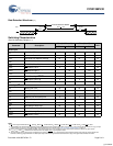
Capacitance
(For all packages)
[8]
Parameter Description Test Conditions Max Unit
C
IN
Input Capacitance T
A
= 25°C, f = 1 MHz,
V
CC
= V
CC(typ)
10 pF
C
OUT
Output Capacitance 10 pF
Note
8. Tested initially and after any design or process changes that may affect these parameters.
9. Full device AC operation requires linear V
CC
ramp from V
DR
to V
CC(min)
> 100 μs or stable at V
CC(min)
> 100 μs.
Thermal Resistance
Parameter Description Test Conditions TSOP I SOIC STSOP Unit
Θ
JA
Thermal Resistance
(Junction to Ambient)
Still Air, soldered on a 3 x 4.5 inch,
two-layer printed circuit board
33.01 48.67 32.56 °C/W
Θ
JC
Thermal Resistance
(Junction to Case)
3.42 25.86 3.59 °C/W
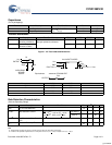
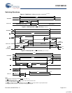
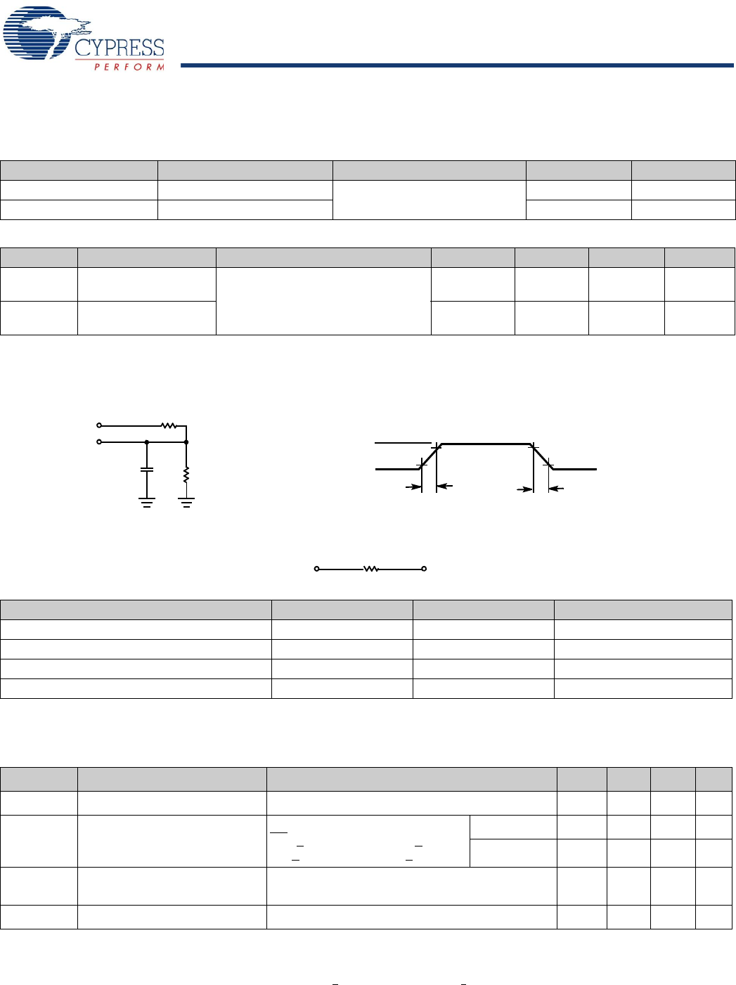
Figure 1. AC Test Loads and Waveforms
V
CC
V
CC
OUTPUT
R2
30 pF
INCLUDING
JIG AND
SCOPE
GND
90%
10%
90%
10%
Rise Time = 1 V/ns
Fall Time = 1 V/ns
OUTPUT V
Equivalent to: THEVENIN EQUIVALENT
ALL INPUT PULSES
R
TH
R1
Parameters 2.50V 3.0V Unit
R1 16667 1103 Ω
R2 15385 1554 Ω
R
TH
8000 645 Ω
V
TH
1.20 1.75 V
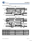
Data Retention Characteristics
(Over the Operating Range)
Parameter Description Conditions Min Typ
[3]
Max Unit
V
DR
V
CC
for Data Retention 1.5 V
I
CCDR
[7]
Data Retention Current V
CC
= 1.5V,
CE
1
> V
CC
− 0.2V or CE
2
< 0.2V,
V
IN
> V
CC
− 0.2V or V
IN
< 0.2V
Ind’l/Auto-A 3 μA
Auto-E 30 μA
t
CDR
[8]
Chip Deselect to Data Retention
Time
0ns
t
R
[9]
Operation Recovery Time t
RC
ns
[+] Feedback