


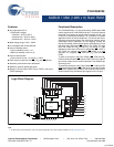
CY62128EV30
Document #: 38-05579 Rev. *D Page 6 of 11
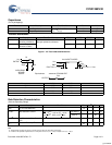
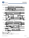
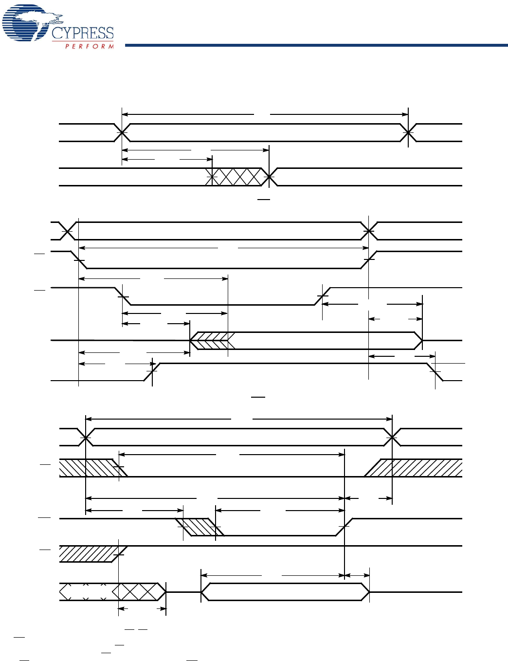
Switching Waveforms
Figure 2. Read Cycle 1 (Address transition controlled)
[15, 16]
Figure 3. Read Cycle No. 2 (OE controlled)
[10, 16, 17]
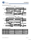
Figure 4. Write Cycle No. 1 (WE controlled)
[10, 15, 18, 19]
PREVIOUS DATA VALID DATA VALID
RC
t
AA
t
OHA
tRC
ADDRESS
DATA OUT
50%
50%
DATA VALID
t
RC
t
ACE
t
DOE
t
LZOE
t
LZCE
t
PU
HIGH IMPEDANCE
t
HZOE
t
HZCE
t
PD
IMPEDANCE
I
CC
I
SB
HIGH
ADDRESS
CE
DATA OUT
V
CC
SUPPLY
CURRENT
OE
DATA VALID
t
HD
t
SD
t
PWE
t
SA
t
HA
t
AW
t
SCE
t
WC
t
HZOE
ADDRESS
CE
WE
DATA IO
OE
NOTE
20
Notes
15.The device is continuously selected. OE
, CE
1
= V
IL
, CE
2
= V
IH
.
16.WE
is HIGH for read cycle.
17.Address valid before or similar to CE
1
transition LOW and CE
2
transition HIGH.
18.Data IO is high impedance if OE
= V
IH
.
19.If CE
1
goes HIGH or CE
2
goes LOW simultaneously with WE HIGH, the output remains in high impedance state.
20.During this period, the IOs are in output state. Do not apply input signals.
[+] Feedback