


CY62136EV30
MoBL
®
Document #: 38-05569 Rev. *B Page 2 of 12
Notes:
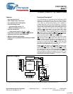
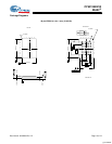
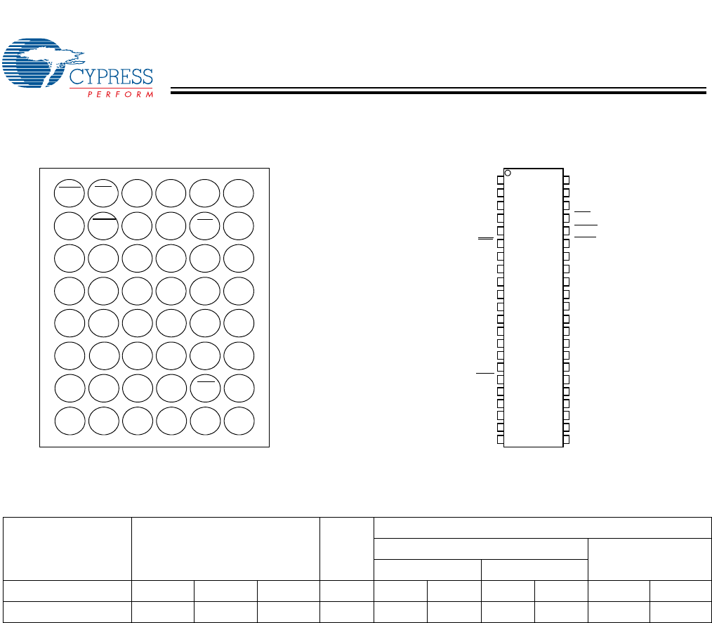
2. NC pins are not connected on the die.
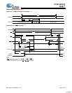
3. Pins D3, H1, G2, and H6 in the BGA package are address expansion pins for 4 Mbit, 8 Mbit, 16 Mbit and 32 Mbit, respectively.
4. Typical values are included for reference only and are not guaranteed or tested. Typical values are measured at V
CC
= V
CC(typ.)
, T
A
= 25°C.
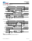
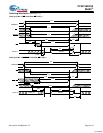
Pin Configuration
[2, 3]
VFBGA (Top View) 44 TSOP II (Top View)
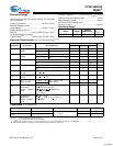
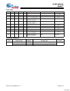
Product Portfolio
[4]
Product V
CC
Range (V)
Speed
(ns)
Power Dissipation
Operating ICC (mA)
Standby I
SB2
(µA)f = 1MHz f = f
max
Min. Typ.
[4]
Max. Typ.
[4]
Max. Typ.
[4]
Max. Typ.
[4]
Max.
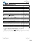
CY62136EV30LL 2.2 3.0 3.6 45 2 2.5 15 20 1 7
WE
A
11
A
10
A
6
A
0
A
3
CE
I/O
10
I/O
8
I/O
9
A
4
A
5
I/O
11
I/O
13
I/O
12
I/O
14
I/O
15
V
SS
A
9
A
8
OE
Vss
A
7
I/O
0
BHE
NC
NC
A
2
A
1
BLE
V
CC
I/O
2
I/O
1
I/O
3
I/O
4
I/O
5
I/O
6
I/O
7
A
15
A
14
A
13
A
12
NC
NC
NC
3
2
6
5
4
1
D
E
B
A
C
F
G
H
A
16
NC
Vcc
WE
1
2
3
4
5
6
7
8
9
10
11
14
31
32
36
35
34
33
37
40
39
38
12
13
41
44
43
42
16
15
29
30
V
CC
A
15
A
14
A
13
A
4
A
3
OE
V
SS
A
5
I/O
15
A
2
CE
I/O
2
I/O
0
I/O
1
BHE
A
1
A
0
18
17
20
19
I/O
3
27
28
25
26
22
21
23
24
V
SS
I/O
6
I/O
4
I/O
5
I/O
7
A
6
A
7
BLE
V
CC
I/O
14
I/O
13
I/O
12
I/O
11
I/O
10
I/O
9
I/O
8
A
8
A
9
A
10
A
11
A
12
NC
NC
A
16
[+] Feedback