CY7C09079V/89V/99V
CY7C09179V/89V/99V
3.3V 32K/64K/128K x 8/9
Synchronous Dual-Port Static RAM
Cypress Semiconductor Corporation • 198 Champion Court • San Jose, CA 95134-1709 • 408-943-2600
Document #: 38-06043 Rev. *C Revised December 10, 2008
Features
■ True Dual-Ported memory cells which enable simultaneous
access of the same memory location
■ 6 Flow-Through and Pipelined devices
■ 32K x 8/9 organizations (CY7C09079V/179V)
■ 64K x 8/9 organizations (CY7C09089V/189V)
■ 128K x 8/9 organizations (CY7C09099V/199V)
■ 3 Modes
■ Flow-Through
■ Pipelined
■ Burst
■ Pipelined output mode on both ports enables fast 100 MHz
operation
■ 0.35-micron CMOS for optimum speed and power
■ High speed clock to data access 6.5[1]/7.5[1]/9/12 ns (max.)
■ 3.3V low operating power
■ Active= 115 mA (typical)
■ Standby= 10 μA (typical)
■ Fully synchronous interface for easier operation
■ Burst counters increment addresses internally
■ Shorten cycle times
■ Minimize bus noise
■ Supported in Flow-Through and Pipelined modes
■ Dual Chip Enables for easy depth expansion
■ Automatic power down
■ Commercial and Industrial temperature ranges
■ Available in 100-pin TQFP
■ Pb-free packages available
Notes
1. See page 6 for Load Conditions.
2. I/O
0
–I/O
7
for x8 devices, I/O
0
–I/O
8
for x9 devices.
3. A
0
–A
14
for 32K, A
0
–A
15
for 64K, and A
0
–A
16
for 128K devices.
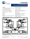
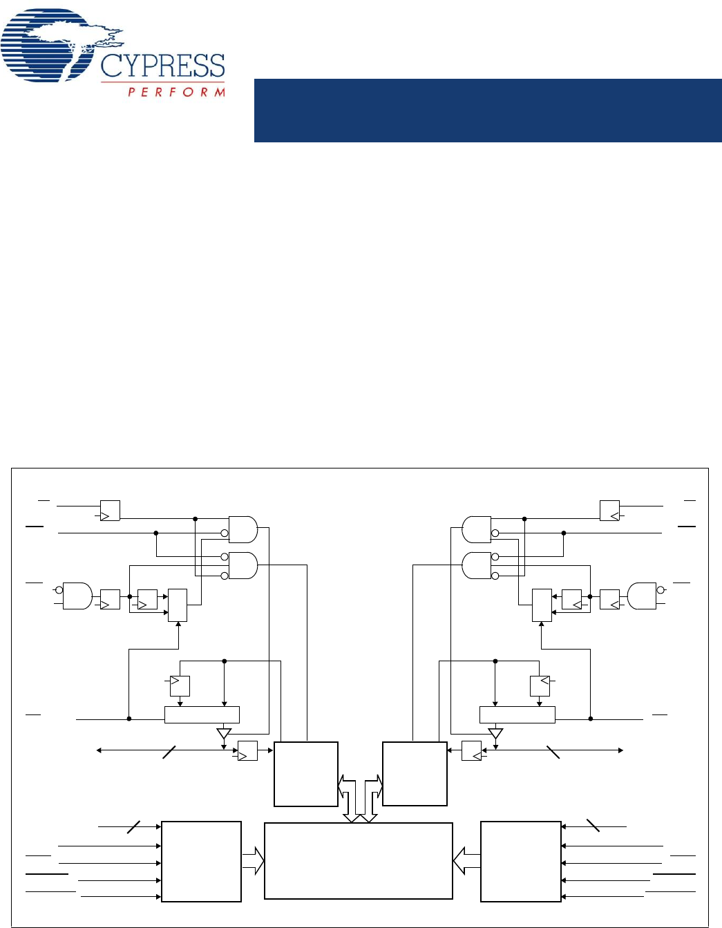
Logic Block Diagram
R/W
L
CE
0L
CE
1L
OE
L
FT/Pipe
L
I/O
0L
–I/O
7/8L
Control
A
0
–A
14/15/16L
CLK
L
ADS
L
CNTEN
L
CNTRST
L
R/W
R
1
0
0/1
CE
0R
CE
1R
OE
R
1
0/1
0
FT/Pipe
R
I/O
0R
–I/O
7/8R
I/O
Control
A
0
–A
14/15/16R
CLK
R
ADS
R
CNTEN
R
CNTRST
R
1
0
0/1
1
0/1
0
I/O
Counter/
Address
Register
Decode
True Dual-Ported
RAM Array
Counter/
Address
Register
Decode
8/9 8/9
[2]
[2]
[3]
[3]
15/16/17
15/16/17
CY7C09079V/89V/99V
CY7C09179V/89V/99V
[+] Feedback


