CY7C09079V/89V/99V
CY7C09179V/89V/99V
Document #: 38-06043 Rev. *C Page 2 of 21
Functional Description
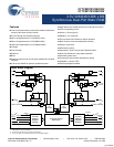
The CY7C09079V/89V/99V and CY7C09179V/89V/99V are
high speed synchronous CMOS 32K, 64K, and 128K x 8/9
dual-port static RAMs. Two ports are provided, permitting
independent, simultaneous access for reads and writes to any
location in memory.
[4]
Registers on control, address, and data
lines enable minimal setup and hold times. In pipelined output
mode, data is registered for decreased cycle time. Clock to data
valid t
CD2
= 6.5 ns
[1]
(pipelined). Flow-through mode can also be
used to bypass the pipelined output register to eliminate access
latency. In flow-through mode, data is available t
CD1
= 18 ns after
the address is clocked into the device. Pipelined output or
flow-through mode is selected via the FT/Pipe pin.
Each port contains a burst counter on the input address register.
The internal write pulse width is independent of the
LOW-to-HIGH transition of the clock signal. The internal write
pulse is self-timed to enable the shortest possible cycle times.
A HIGH on CE
0
or LOW on CE
1
for one clock cycle powers down
the internal circuitry to reduce the static power consumption. The
use of multiple Chip Enables enables easier banking of multiple
chips for depth expansion configurations. In the pipelined mode,
one cycle is required with CE
0
LOW and CE
1
HIGH to reactivate
the outputs.
Counter enable inputs are provided to stall the operation of the
address input and use the internal address generated by the
internal counter for fast interleaved memory applications. A
port’s burst counter is loaded with the port’s Address Strobe
(ADS
). When the port’s Count Enable (CNTEN) is asserted, the
address counter increments on each LOW-to-HIGH transition of
that port’s clock signal. This reads/writes one word from/into
each successive address location until CNTEN
is deasserted.
The counter can address the entire memory array and loops
back to the start. Counter Reset (CNTRST
) is used to reset the
burst counter.
All parts are available in 100-pin Thin Quad Plastic Flatpack
(TQFP) packages.
Pin Configurations
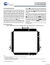
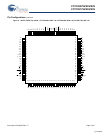
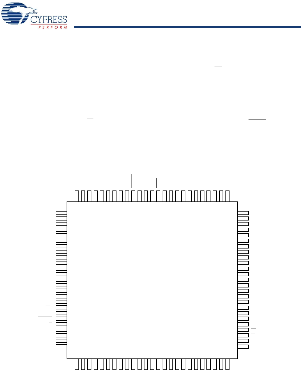
Figure 1. 100-Pin TQFP (Top View) - CY7C09099V (128K x 8), CY7C09089V (64K x 8),CY7C09079V (32K x 8)
Notes
4. When writing simultaneously to the same location, the final value cannot be guaranteed.
5. This pin is NC for CY7C09079V.
6. This pin is NC for CY7C09079V and CY7C09089V.
7. For CY7C09079V and CY7C09089V, pin #23 connected to V
CC
is pin compatible with an IDT 5V x8 pipelined device; connecting pin #23 and #53 to GND is pin
compatible with an IDT 5V x16 flow-through device.
1
3
2
92 91 90 848587 868889 83 82 81 7678 77798093949596979899100
59
60
61
67
66
64
65
63
62
68
69
70
75
73
74
72
71
NC
NC
A7R
A8R
A9R
A10R
A15R
A12R
A14R
GND
NC
NC
CE
0R
A13R
A11R
NC
NC
CE1R
CNTRST
R
R/WR
OER
FT
/PIPER
GND
NC
A16R
58
57
56
55
54
53
52
51
NC
NC
A7L
A8L
A9L
A10L
A15L
A12L
A14L
VCC
NC
NC
CE0L
A13L
A11L
NC
NC
CE1L
CNTRSTL
R/W
L
OEL
FT
/PIPEL
NC
NC
A16L
17
16
15
9
10
12
11
13
14
8
7
6
4
5
18
19
20
21
22
23
24
25
NC
NC
A6L
A5L
A4L
A3L
CLKL
A1L
CNTENL
GND
ADSR
A0R
A1R
A0L
A2L
CLKR
CNTENR
A2R
A3R
A4R
A5R
A6R
NC
NC
ADSL
34 35 36 424139 403837 43 44 45 5048 494746
NC
NC
NC
I/O7R
I/O6R
I/O5R
I/01R
I/O3R
I/O2R
GND
VCC
GND
I/O2L
VCC
I/O4R
I/O0L
I/O1L
I/O3L
I/O4L
I/O5L
I/O6L
I/O7L
NC
GND
I/O0R
3332313029282726
[5]
[5]
[6]
[6]
[7]
[7]
[+] Feedback


