CY7C09079V/89V/99V
CY7C09179V/89V/99V
Document #: 38-06043 Rev. *C Page 4 of 21
Notes
8. This pin is NC for CY7C09179V.
9. This pin is NC for CY7C09179V and CY7C09189V
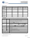
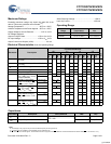
Selection Guide
Description
CY7C09079V/89V/99V
CY7C09179V/89V/99V-6
[1]
CY7C09079V/89V/99V
CY7C09179V/89V/99V-7
[1]
CY7C09079V/89V/99V
CY7C09179V/89V/99V
-9
CY7C09079V/89V/99V
CY7C09179V/89V/99V
-12
f
MAX2
(MHz)
(Pipelined)
100 83 67 50
Max. Access Time
(ns) (Clock to Data,
Pipelined)
6.5 7.5 9 12
Typical Operating
Current I
CC
(mA)
175 155 135 115
Typical Standby
Current for I
SB1
(mA) (Both Ports
TTL Level)
25 25 20 20
Typical Standby
Current for I
SB3
(μA) (Both Ports
CMOS Level)
10 μA 10 μA10 μA 10 μA
Pin Definitions
Left Port Right Port Description
A
0L
–A
16L
A
0R
–A
16R
Address Inputs (A
0
–A
14
for 32K; A
0
–A
15
for 64K; and A
0
–A
16
for 128K devices).
ADS
L
ADS
R
Address Strobe Input. Used as an address qualifier. This signal should be asserted LOW to
access the part using an externally supplied address. Asserting this signal LOW also loads
the burst counter with the address present on the address pins.
CE
0L
,CE
1L
CE
0R
,CE
1R
Chip Enable Input. To select either the left or right port, both CE
0
AND CE
1
must be asserted
to their active states (CE
0
≤ V
IL
and CE
1
≥ V
IH
).
CLK
L
CLK
R
Clock Signal. This input can be free running or strobed. Maximum clock input rate is f
MAX
.
CNTEN
L
CNTEN
R
Counter Enable Input. Asserting this signal LOW increments the burst address counter of its
respective port on each rising edge of CLK. CNTEN
is disabled if ADS or CNTRST are
asserted LOW.
CNTRST
L
CNTRST
R
Counter Reset Input. Asserting this signal LOW resets the burst address counter of its
respective port to zero. CNTRST
is not disabled by asserting ADS or CNTEN.
I/O
0L
–I/O
8L
I/O
0R
–I/O
8R
Data Bus Input/Output (I/O
0
–I/O
7
for x8 devices; I/O
0
–I/O
8
for x9 devices).
OE
L
OE
R
Output Enable Input. This signal must be asserted LOW to enable the I/O data pins during
read operations.
R/W
L
R/W
R
Read/Write Enable Input. This signal is asserted LOW to write to the dual port memory array.
For read operations, assert this pin HIGH.
FT/PIPE
L
FT/PIPE
R
Flow-Through/Pipelined Select Input. For flow-through mode operation, assert this pin LOW.
For pipelined mode operation, assert this pin HIGH.
GND Ground Input.
NC No Connect.
V
CC
Power Input.
[+] Feedback


