CY7C1034DV33
Document Number: 001-08351 Rev. *C Page 4 of 9
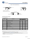
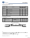
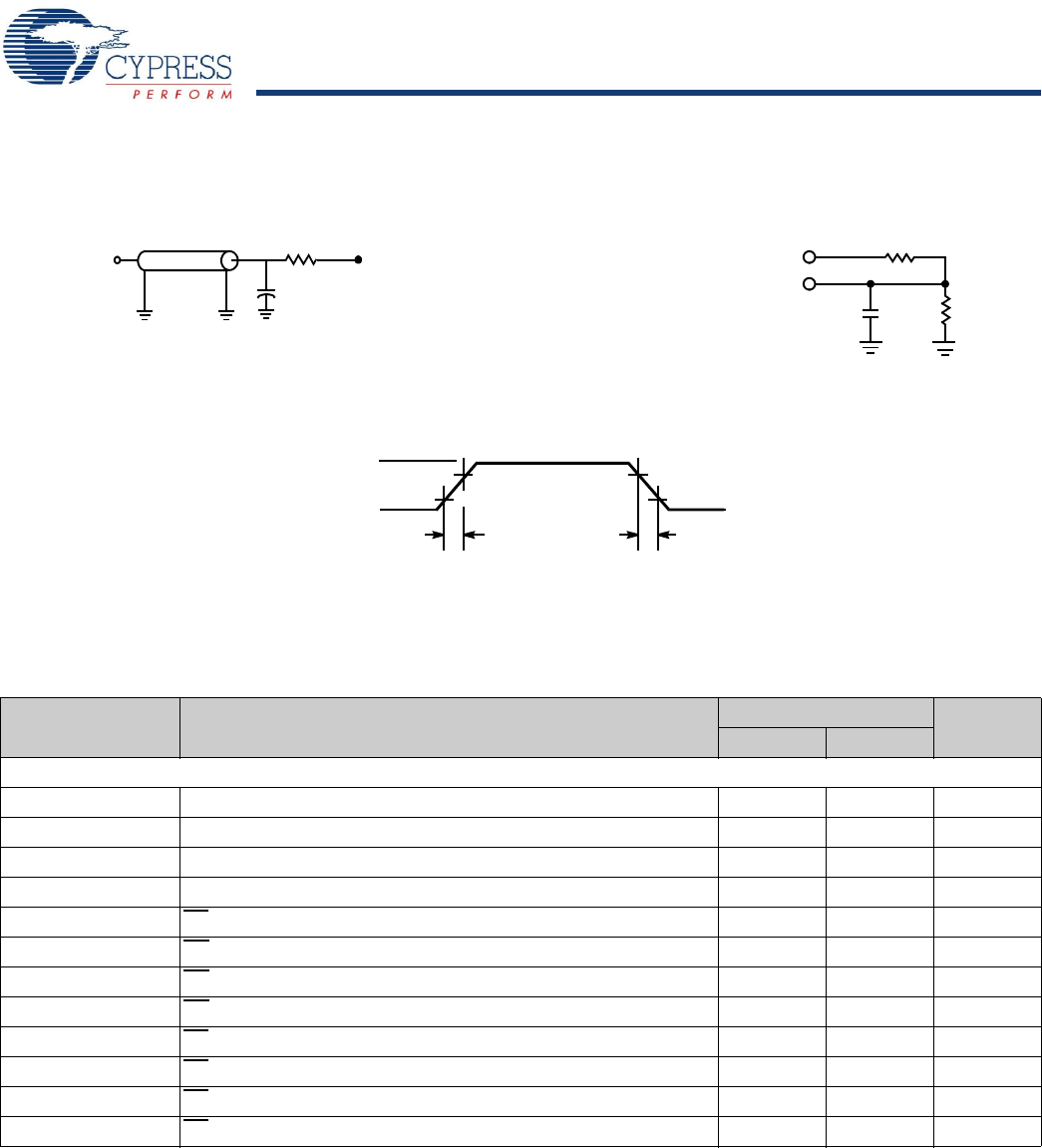
Figure 2. AC Test Loads and Waveform
[4]
AC Switching Characteristics
Over the operating range
[5]
Parameter Description
–10
Unit
Min Max
Read Cycle
t
power
[6]
V
CC
(Typical) to the First Access 100 μs
t
RC
Read Cycle Time 10 ns
t
AA
Address to Data Valid 10 ns
t
OHA
Data Hold from Address Change 3 ns
t
ACE
CE
Active LOW to Data Valid
[3]
10 ns
t
DOE
OE LOW to Data Valid 5 ns
t
LZOE
OE LOW to Low Z
[7]
1ns
t
HZOE
OE HIGH to High Z
[7]
5ns
t
LZCE
CE
Active LOW to Low Z
[3, 7]
3ns
t
HZCE
CE Deselect HIGH to High Z
[3, 7]
5ns
t
PU
CE
Active LOW to Power Up
[3, 8]
0ns
t
PD
CE Deselect HIGH to Power Down
[3, 8]
10 ns
90%
10%
3.0V
GND
90%
10%
All input pulses
3.3V
OUTPUT
5 pF*
(a)
(b)
R1 317 Ω
R2
351Ω
Fall Time:> 1V/ns
(c)
OUTPUT
50Ω
Z
0
= 50Ω
V
TH
= 1.5V
30 pF*
*Capacitive Load consists of all
components of the test environment
Rise Time > 1V/ns
*Including jig
and scope
Notes
4. Valid SRAM operation does not occur until the power supplies reach the minimum operating V
DD
(3.0V). 100 μs (t
power
) after reaching the minimum operating V
DD
,
normal SRAM operation begins including reduction in V
DD
to the data retention (V
CCDR
, 2.0V) voltage.
5. Test conditions assume signal transition time of 3 ns or less, timing reference levels of 1.5V, and input pulse levels of 0 to 3.0V. Test conditions for the read cycle use
output loading as shown in part a) of the AC Test Loads and Waveform
[4]
, unless specified otherwise.
6. t
POWER
gives the minimum amount of time that the power supply is at typical V
CC
values until the first memory access is performed.
7. t
HZOE
, t
HZCE
, t
HZWE
, t
LZOE
, t
LZCE
, and t
LZWE
are specified with a load capacitance of 5 pF as in part (b) of AC Test Loads. Transition is measured ±200 mV from steady
state voltage.
8. These parameters are guaranteed by design and are not tested.
[+] Feedback


