CY7C1292DV18
CY7C1294DV18
Document #: 001-00350 Rev. *A Page 23 of 23
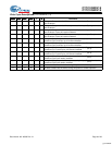
Document History Page
Document Title: CY7C1292DV18/CY7C1294DV18 9-Mbit QDR- II™ SRAM 2-Word Burst Architecture
Document Number: 001-00350
REV. ECN No. Issue Date
Orig. of
Change Description of Change
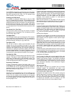
** 380737 See ECN SYT New data sheet
*A 485631 See ECN NXR Converted from Preliminary to Final
Removed 300MHz Speed Bin.
Changed address of Cypress Semiconductor Corporation on Page# 1 from
“3901 North First Street” to “198 Champion Court”
Changed C/C
Pin Description in the features section and Pin Description.
Modified the ZQ Definition from Alternately, this pin can be connected directly
to V
DD
to Alternately, this pin can be connected directly to V
DDQ.
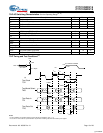
Changed t
TH
and t
TL
from 40 ns to 20 ns, changed t
TMSS
, t
TDIS
, t
CS
, t
TMSH
,
t
TDIH
, t
CH
from
10 ns to 5 ns and changed t
TDOV
from 20 ns to 10 ns in TAP
AC Switching Characteristics table
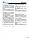
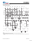
Added power-up sequence details and waveforms.
Added foot notes #15 and 16 on page# 18.
Included Maximum Ratings for Supply Voltage on V
DDQ
Relative to GND
Changed the Maximum rating of Ambient Temperature with Power Applied
from –10°C to +85°C to –55°C to +125°C
Changed the Maximum Ratings for DC Input Voltage from V
DDQ
to V
DD.
Changed the description of I
X
from Input Load Current to Input Leakage
Current on page# 13.
Modified the I
DD
and I
SB
values
Modified test condition in Footnote #20 on page# 19 from V
DDQ
< V
DD
to
V
DDQ
< V
DD.
Changed the Min. Value of t
SC
and t
HC
from 0.5ns to 0.35ns for 250 MHz and
0.6ns to 0.4ns for 200 MHz speed bins.
Changed the description of t
SA
from K Clock Rise to Clock (K/K) Rise.
Changed the description of t
SC
and
t
HC
from Clock (K and K) Rise to K Clock
Rise.
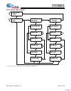
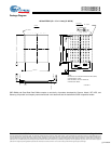
Replaced Package Name column with Package Diagram in the Ordering
Information table.
Updated the Ordering Information Table.
[+] Feedback


