CY7C1292DV18
CY7C1294DV18
Document #: 001-00350 Rev. *A Page 6 of 23
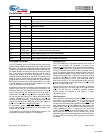
Byte Write Operations
Byte Write operations are supported by the CY7C1292DV18.
A Write operation is initiated as described in the Write Opera-
tions section above. The bytes that are written are determined
by BWS
0
and BWS
1
, which are sampled with each 18-bit data
word. Asserting the appropriate Byte Write Select input during
the data portion of a Write will allow the data being presented
to be latched and written into the device. Deasserting the Byte
Write Select input during the data portion of a write will allow
the data stored in the device for that byte to remain unaltered.
This feature can be used to simplify Read/Modify/Write opera-
tions to a Byte Write operation.
Single Clock Mode
The CY7C1292DV18 can be used with a single clock that
controls both the input and output registers. In this mode, the
device will recognize only a single pair of input clocks (K and
K
) that control both the input and output registers. This
operation is identical to the operation if the device had zero
skew between the K/K
and C/C clocks. All timing parameters
remain the same in this mode. To use this mode of operation,
the user must tie C and C HIGH at power on. This function is
a strap option and not alterable during device operation.
Concurrent Transactions
The Read and Write ports on the CY7C1292DV18 operate
completely independently of one another. Since each port
latches the address inputs on different clock edges, the user
can Read or Write to any location, regardless of the trans-
action on the other port. Also, reads and writes can be started
in the same clock cycle. If the ports access the same location
at the same time, the SRAM will deliver the most recent infor-
mation associated with the specified address location. This
includes forwarding data from a Write cycle that was initiated
on the previous K clock rise.
Depth Expansion
The CY7C1292DV18 has a Port Select input for each port.
This allows for easy depth expansion. Both Port Selects are
sampled on the rising edge of the Positive Input Clock only (K).
Each port select input can deselect the specified port.
Deselecting a port will not affect the other port. All pending
transactions (Read and Write) will be completed prior to the
device being deselected.
Programmable Impedance
An external resistor, RQ, must be connected between the ZQ
pin on the SRAM and V
SS
to allow the SRAM to adjust its
output driver impedance. The value of RQ must be 5x the
value of the intended line impedance driven by the SRAM. The
allowable range of RQ to guarantee impedance matching with
a tolerance of ±15% is between 175Ω and 350Ω
, with
V
DDQ
= 1.5V.The output impedance is adjusted every 1024
cycles upon power-up to account for drifts in supply voltage
and temperature.
Echo Clocks
Echo clocks are provided on the QDR-II to simplify data
capture on high-speed systems. Two echo clocks are
generated by the QDR-II. CQ is referenced with respect to C
and CQ
is referenced with respect to C. These are
free-running clocks and are synchronized to the output clock
(C/C
) of the QDR-II. In the single clock mode, CQ is generated
with respect to K and CQ
is generated with respect to K. The
timings for the echo clocks are shown in the AC Timing table.
DLL
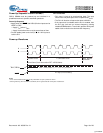
These chips utilize a Delay Lock Loop (DLL) that is designed
to function between 80 MHz and the specified maximum clock
frequency. During power-up, when the DOFF
is tied HIGH, the
DLL gets locked after 1024 cycles of stable clock. The DLL can
also be reset by slowing or stopping the input clock K and K
for a minimum of 30 ns. However, it is not necessary for the
DLL to be specifically reset in order to lock the DLL to the
desired frequency. The DLL will automatically lock 1024 clock
cycles after a stable clock is presented.the DLL may be
disabled by applying ground to the DOFF
pin. For information
refer to the application note “DLL Considerations in
QDRII/DDRII/QDRII+/DDRII+”.
[+] Feedback


