


CY7C1298H
Document #: 38-05665 Rev. *B Page 10 of 16
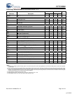
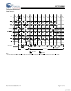
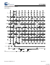
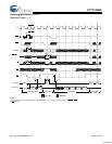
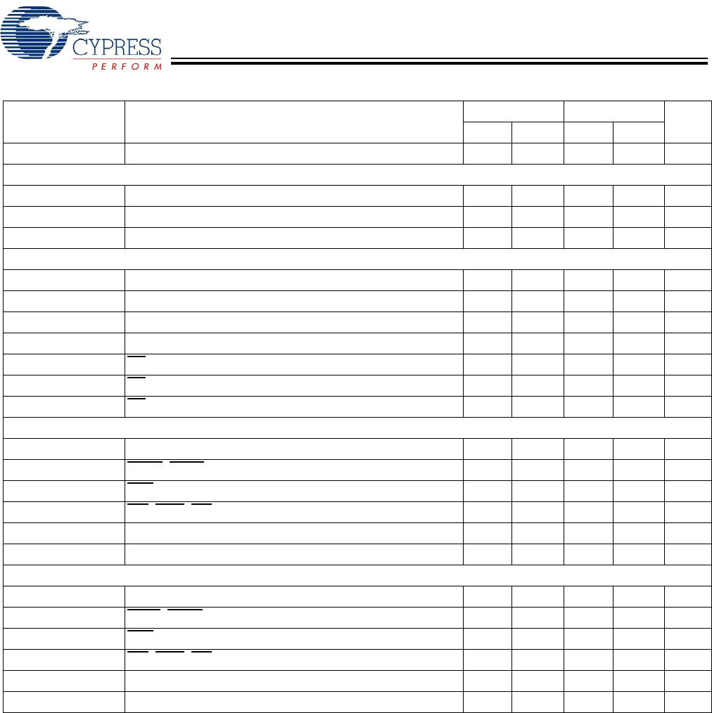
Switching Characteristics Over the Operating Range
[14, 15]
Parameter Description
166 MHz 133 MHz
UnitMin. Max. Min. Max.
t
POWER
V
DD
(Typical) to the first Access
[10]
11ms
Clock
t
CYC
Clock Cycle Time 6.0 7.5 ns
t
CH
Clock HIGH 2.5 3.0 ns
t
CL
Clock LOW 2.5 3.0 ns
Output Times
t
CO
Data Output Valid After CLK Rise 3.5 4.0 ns
t
DOH
Data Output Hold After CLK Rise 1.5 1.5 ns
t
CLZ
Clock to Low-Z
[11, 12, 13]
00ns
t
CHZ
Clock to High-Z
[11, 12, 13]
3.5 4.0 ns
t
OEV
OE LOW to Output Valid 3.5 4.0 ns
t
OELZ
OE LOW to Output Low-Z
[11, 12, 13]
00ns
t
OEHZ
OE HIGH to Output High-Z
[11, 12, 13]
3.5 4.0 ns
Set-up Times
t
AS
Address Set-up Before CLK Rise 1.5 1.5 ns
t
ADS
ADSC, ADSP Set-up Before CLK Rise 1.5 1.5 ns
t
ADVS
ADV Set-up Before CLK Rise 1.5 1.5 ns
t
WES
GW, BWE, BW
[A:B]
Set-up Before CLK Rise 1.5 1.5 ns
t
DS
Data Input Set-up Before CLK Rise 1.5 1.5 ns
t
CES
Chip Enable Set-up Before CLK Rise 1.5 1.5 ns
Hold Times
t
AH
Address Hold After CLK Rise 0.5 0.5 ns
t
ADH
ADSP, ADSC Hold After CLK Rise 0.5 0.5 ns
t
ADVH
ADV Hold After CLK Rise 0.5 0.5 ns
t
WEH
GW, BWE, BW
[A:B]
Hold After CLK Rise 0.5 0.5 ns
t
DH
Data Input Hold After CLK Rise 0.5 0.5 ns
t
CEH
Chip Enable Hold After CLK Rise 0.5 0.5 ns
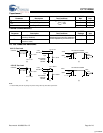
Notes:
10.This part has a voltage regulator internally; tpower is the time that the power needs to be supplied above V
DD
minimum initially before a read or write operation
can be initiated.
11. t
CHZ
, t
CLZ
,t
OELZ
, and t
OEHZ
are specified with AC test conditions shown in part (b) of AC Test Loads. Transition is measured ± 200 mV from steady-state voltage.
12.At any given voltage and temperature, t
OEHZ
is less than t
OELZ
and t
CHZ
is less than t
CLZ
to eliminate bus contention between SRAMs when sharing the same
data bus. These specifications do not imply a bus contention condition, but reflect parameters guaranteed over worst case user conditions. Device is designed
to achieve High-Z prior to Low-Z under the same system conditions.
13.This parameter is sampled and not 100% tested.
14.Timing reference level is 1.5V when V
DDQ
= 3.3V and is 1.25V when V
DDQ
= 2.5V.
15.Test conditions shown in (a) of AC Test Loads unless otherwise noted.
[+] Feedback