


CY7C1298H
Document #: 38-05665 Rev. *B Page 8 of 16
Maximum Ratings
(Above which the useful life may be impaired. For user guide-
lines, not tested.)
Storage Temperature ................................... –65°C to + 150°
Ambient Temperature with
Power Applied............................................–55°C to + 125°C
Supply Voltage on V
DD
Relative to GND.......–0.5V to + 4.6V
Supply Voltage on V
DDQ
Relative to GND .....–0.5V to + V
DD
DC Voltage Applied to Outputs
in tri-state............................................ –0.5V to V
DDQ
+ 0.5V
DC Input Voltage ...................................–0.5V to V
DD
+ 0.5V
Current into Outputs (LOW)......................................... 20 mA
Static Discharge Voltage...........................................> 2001V
(per MIL-STD-883,Method 3015)
Latch -up Current....................................................> 200 mA
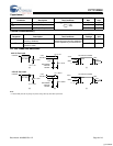
Operating Range
Range
Ambient
Temperature (T
A
)V
DD
V
DDQ
Com’l 0°C to +70°C 3.3V −5%/+10% 2.5V −5%
to V
DD
Ind’l –40°C to +85°C
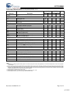
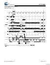
Electrical Characteristics Over the Operating Range
[7,8]
Parameter Description Test Conditions Min. Max. Unit
V
DD
Power Supply Voltage 3.135 3.6 V
V
DDQ
I/O Supply Voltage for 3.3V I/O 3.135 V
DD
V
for 2.5V I/O 2.375 2.625 V
V
OH
Output HIGH Voltage for 3.3V I/O, I
OH
= –4.0 mA 2.4 V
for 2.5V I/O, I
OH
= –1.0 mA 2.0 V
V
OL
Output LOW Voltage for 3.3V I/O, I
OL
= 8.0 mA 0.4 V
for 2.5V I/O, I
OL
= 1.0 mA 0.4 V
V
IH
Input HIGH Voltage
[7]
for 3.3V I/O 2.0 V
DD
+ 0.3V V
for 2.5V I/O 1.7 V
DD
+ 0.3V V
V
IL
Input LOW Voltage
[7]
for 3.3V I/O –0.3 0.8 V
for 2.5V I/O –0.3 0.7 V
I
X
Input Leakage Current
except ZZ and MODE
GND ≤ V
I
≤ V
DDQ
–5 5 µA
Input Current of MODE Input = V
SS
–30 µA
Input = V
DD
5 µA
Input Current of ZZ Input = V
SS
–5 µA
Input = V
DD
30 µA
I
OZ
Output Leakage Current GND ≤ V
I
≤ V
DDQ,
Output Disabled –5 5 µA
I
DD
V
DD
Operating Supply
Current
V
DD
= Max., I
OUT
= 0 mA,
f = f
MAX
= 1/t
CYC
6-ns cycle, 166 MHz 240 mA
7.5-ns cycle, 133 MHz 225 mA
I
SB1
Automatic CS
Power-down
Current—TTL Inputs
V
DD
= Max., Device Deselected,
V
IN
≥ V
IH
or V
IN
≤ V
IL
,
f = f
MAX
= 1/t
CYC
6-ns cycle, 166 MHz 100 mA
7.5-ns cycle, 133 MHz 90 mA
I
SB2
Automatic CS
Power-down
Current—CMOS Inputs
V
DD
= Max., Device Deselected,
V
IN
≤ 0.3V or
V
IN
> V
DDQ
– 0.3V, f = 0
All speeds 40 mA
I
SB3
Automatic CS
Power-down
Current—CMOS Inputs
V
DD
= Max., Device Deselected,
or V
IN
≤ 0.3V or
V
IN
> V
DDQ
– 0.3V,
f = f
MAX
= 1/t
CYC
6-ns cycle, 166 MHz 85 mA
7.5-ns cycle, 133 MHz 75 mA
I
SB4
Automatic CS
Power-down
Current—TTL Inputs
V
DD
= Max., Device Deselected,
V
IN
≥ V
IH
or V
IN
≤ V
IL
, f = 0
All speeds 45 mA
Notes:
7. Overshoot: V
IH
(AC) < V
DD
+1.5V (Pulse width less than t
CYC
/2), undershoot: V
IL
(AC)> –2V (Pulse width less than t
CYC
/2).
8. Power-up: Assumes a linear ramp from 0V to V
DD
(min.) within 200 ms. During this time V
IH
< V
DD
and V
DDQ
< V
DD
.
[+] Feedback