CY7C1302DV25
Document #: 38-05625 Rev. *A Page 3 of 18
Introduction
Functional Overview
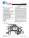
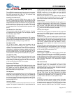
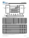
The CY7C1302DV25 is a synchronous pipelined Burst SRAM
equipped with both a Read port and a Write port. The Read
port is dedicated to Read operations and the Write port is
dedicated to Write operations. Data flows into the SRAM
through the Write port and out through the Read port. These
devices multiplex the address inputs in order to minimize the
number of address pins required. By having separate Read
and Write ports, the QDR-I completely eliminates the need to
“turn-around” the data bus and avoids any possible data
contention, thereby simplifying system design. 38-05625
Accesses for both ports are initiated on the rising edge of the
Positive Input Clock (K). All synchronous input timing is refer-
enced from the rising edge of the input clocks (K and K
) and
all output timing is referenced to the output clocks (C and C,
or K and K when in single clock mode).
All synchronous data inputs (D
[17:0]
) pass through input
registers controlled by the input clocks (K and K
). All
synchronous data outputs (Q
[17:0]
) pass through output
registers controlled by the rising edge of the output clocks (C
and C
, or K and K when in single clock mode).
All synchronous control (RPS
, WPS, BWS
[1:0]
) inputs pass
through input registers controlled by the rising edge of input
clocks (K and K
).
Read Operations
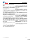
The CY7C1302DV25 is organized internally as 2 arrays of
256K x 18. Accesses are completed in a burst of two
sequential 18-bit data words. Read operations are initiated by
asserting RPS
active at the rising edge of the positive input
clock (K). The address is latched on the rising edge of the K
clock. Following the next K clock rise the corresponding lower
order 18-bit word of data is driven onto the Q
[17:0]
using C as
the output timing reference. On the subsequent rising edge of
C
the higher order data word is driven onto the Q
[17:0]
. The
requested data will be valid 2.5 ns from the rising edge of the
output clock (C and C
, or K and K when in single clock mode,
167-MHz device).
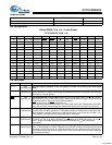
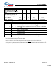
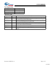
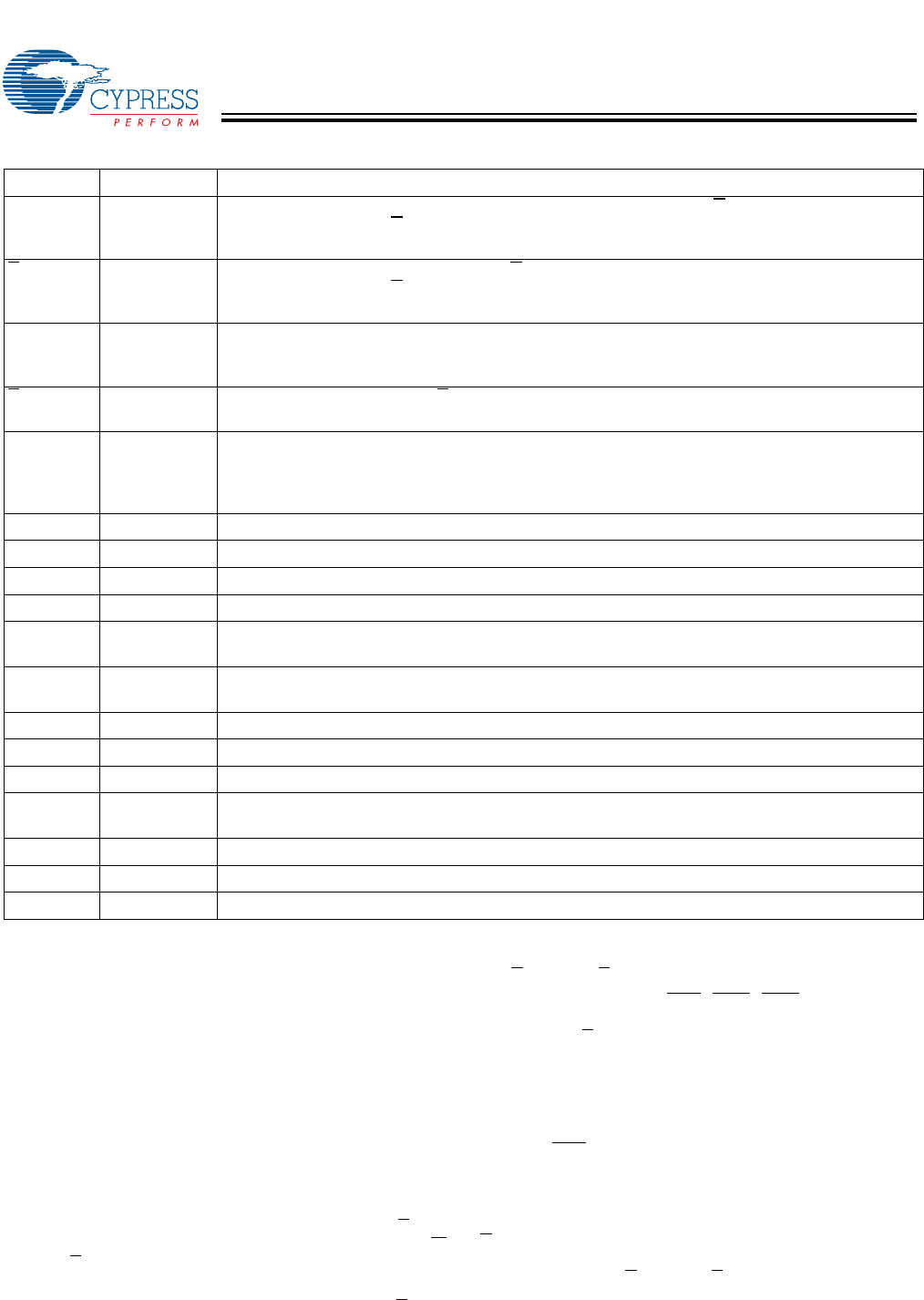
C Input-
Clock
Positive Input Clock for Output Data. C is used in conjunction with C
to clock out the Read data
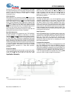
from the device. C and C
can be used together to deskew the flight times of various devices on
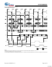
the board back to the controller. See application example for further details.
C Input-Clock Negative Input Clock for Output Data. C is used in conjunction with C to clock out the Read data
from the device. C and C
can be used together to deskew the flight times of various devices on
the board cack to the controller. See application example for further details.
K Input-Clock Positive Input Clock Input. The rising edge of K is used to capture synchronous inputs to the
device and to drive out data through Q
[17:0]
when in single clock mode. All accesses are initiated
on the rising edge of K.
K
Input-Clock Negative Input Clock Input. K is used to capture synchronous inputs being presented to the
device and to drive out data through Q
[17:0]
when in single clock mode.
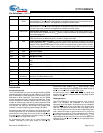
ZQ Input Output Impedance Matching Input. This input is used to tune the device outputs to the system
data bus impedance. Q
[17:0]
output impedance is set to 0.2 x RQ, where RQ is a resistor connected
between ZQ and ground. Alternately, this pin can be connected directly to V
DDQ
, which enables
the minimum impedance mode. This pin cannot be connected directly to GND or left unconnected.
TDO Output TDO for JTAG.
TCK Input TCK pin for JTAG.
TDI Input TDI pin for JTAG.
TMS Input TMS pin for JTAG.
NC/18M N/A Address expansion for 18M. This is not connected to the die and so can be tied to any voltage
level.
NC/36M N/A Address expansion for 36M. This is not connected to the die and so can be tied to any voltage
level.
GND/72M Input Address expansion for 72M. This must be tied LOW.
GND/144M Input Address expansion for 144M. This must be tied LOW.
NC N/A Not connected to the die. Can be tied to any voltage level.
V
REF
Input-
Reference
Reference Voltage Input. Static input used to set the reference level for HSTL inputs and Outputs
as well as AC measurement points.
V
DD
Power Supply Power supply inputs to the core of the device.
V
SS
Ground Ground for the device.
V
DDQ
Power Supply Power supply inputs for the outputs of the device.
Pin Definitions (continued)
Name I/O Description
[+] Feedback


