CY7C1310AV18
CY7C1312AV18
CY7C1314AV18
PRELIMINARY
Document #: 38-05497 Rev. *A Page 4 of 21
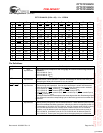
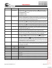
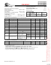
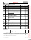
Pin Definitions
Pin Name I/O Pin Description
D
[x:0]
Input-
Synchronous
Data input signals, sampled on the rising edge of K and K clocks during valid write
operations.
CY7C1310AV18 - D
[7:0]
CY7C1312AV18 - D
[17:0]
CY7C1314AV18 - D
[35:0]
WPS Input-
Synchronous
Write Port Select, active LOW. Sampled on the rising edge of the K clock. When
asserted active, a write operation is initiated. Deasserting will deselect the Write port.
Deselecting the Write port will cause D
[x:0]
to be ignored.
BWS
0
, BWS
1
,
BWS
2
, BWS
3
Input-
Synchronous
Byte Write Select 0, 1, 2 and 3 − active LOW. Sampled on the rising edge of the K and
K
clocks during write operations. Used to select which byte is written into the device
during the current portion of the write operations. Bytes not written remain unaltered.
CY7C1310AV18 − BWS
0
controls D
[3:0]
and BWS
1
controls D
[7:4]
.
CY7C1312AV18 − BWS
0
controls D
[8:0]
and BWS
1
controls D
[17:9].
CY7C1314AV18 − BWS
0
controls D
[8:0]
, BWS
1
controls D
[17:9]
, BWS
2
controls D
[26:18]
and BWS
3
controls D
[35:27].
All the Byte Write Selects are sampled on the same edge as the data. Deselecting a Byte
Write Select will cause the corresponding byte of data to be ignored and not written into
the device.
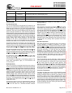
A Input-
Synchronous
Address Inputs. Sampled on the rising edge of the K (read address) and K
(write
address) clocks during active read and write operations. These address inputs are multi-
plexed for both Read and Write operations. Internally, the device is organized as 2M x 8
(2 arrays each of 1M x 8) for CY7C1310AV18, 1M x 18 (2 arrays each of 512K x 18) for
CY7C1312AV18 and 512K x 36 (2 arrays each of 256K x 36) for CY7C1314AV18.
Therefore, only 20 address inputs are needed to access the entire memory array of
CY7C1310AV18, 19 address inputs for CY7C1312AV18 and 18 address inputs for
CY7C1314AV18. These inputs are ignored when the appropriate port is deselected.
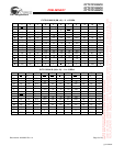
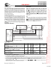
Pin Configurations (continued)
23
4
567
1
A
B
C
D
E
F
G
H
J
K
L
M
N
P
R
A
CQ
Q27
D27
D28
D34
DOFF
Q33
V
SS
/288M NC/72M
BWS
2
K
WPS
BWS
1
Q18
D18
Q30
D31
D33
TDO
Q28
D29
D22
D32
Q34
Q31
TCK
D35
D19
A
BWS
3
K
BWS
0
V
SS
AAA
Q19 V
SS
V
SS
V
SS
V
SS
V
DD
A
V
SS
V
SS
V
SS
V
DD
Q20
D21
V
DDQ
D23
Q23
D25
Q25
Q26
A
V
DDQ
V
SS
V
DDQ
V
DD
V
DD
Q22 V
DDQ
V
DD
V
DDQ
V
DD
V
DDQ
V
DD
V
SS
V
DD
V
DDQ
V
DDQ
V
SS
V
SS
V
SS
V
SS
A
A
C
V
SS
A
A
A
D20 V
SS
Q29
V
SS
Q21
D30
V
REF
V
SS
V
DD
V
SS
V
SS
A
V
SS
C
Q32
Q24
Q35
D26
D24
V
DD
A
891011
Q0
NC/36M V
SS
/144M
RPS
CQ
A D17
Q17
Q8
V
SS
D16 Q7 D8
Q16
V
SS
D15
Q6
D5
D9
Q14
V
REF
Q11
Q3
V
DDQ
Q15
V
DDQ
D14 Q5
V
DDQ
VDDQ
V
DDQ
D4V
DDQ
D12
Q4
Q12
V
DDQ
V
DDQ
D11
V
SS
D10 D2
Q10
TDITMS
V
SS
A
Q9
A
D7
D6
D13
ZQ
D3
Q2
D1
Q1
D0
Q13
A
CY7C1314AV18 (512k × 36) – 11 × 15 BGA
[+] Feedback


