CY7C1310AV18
CY7C1312AV18
CY7C1314AV18
PRELIMINARY
Document #: 38-05497 Rev. *A Page 7 of 21
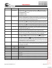
Depth Expansion
The CY7C1312AV18 has a Port Select input for each port.
This allows for easy depth expansion. Both Port Selects are
sampled on the rising edge of the Positive Input Clock only (K).
Each port select input can deselect the specified port.
Deselecting a port will not affect the other port. All pending
transactions (Read and Write) will be completed prior to the
device being deselected.
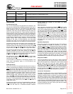
Programmable Impedance
An external resistor, RQ, must be connected between the ZQ
pin on the SRAM and V
SS
to allow the SRAM to adjust its
output driver impedance. The value of RQ must be 5x the
value of the intended line impedance driven by the SRAM. The
allowable range of RQ to guarantee impedance matching with
a tolerance of ±15% is between 175Ω and 350Ω
, with
V
DDQ
= 1.5V.The output impedance is adjusted every 1024
cycles upon powerup to account for drifts in supply voltage and
temperature.
Echo Clocks
Echo clocks are provided on the QDR-II to simplify data
capture on high-speed systems. Two echo clocks are
generated by the QDR-II. CQ is referenced with respect to C
and CQ
is referenced with respect to C. These are
free-running clocks and are synchronized to the output
clock(C/C
) of the QDR-II. In the single clock mode, CQ is
generated with respect to K and CQ
is generated with respect
to K
. The timings for the echo clocks are shown in the AC
Timing table.
DLL
These chips utilize a Delay Lock Loop (DLL) that is designed
to function between 80 MHz and the specified maximum clock
frequency. The DLL may be disabled by applying ground to the
DOFF
pin. The DLL can also be reset by slowing the cycle time
of input clocks K and K
to greater than 30 ns.
\
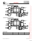
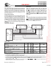
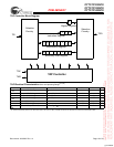
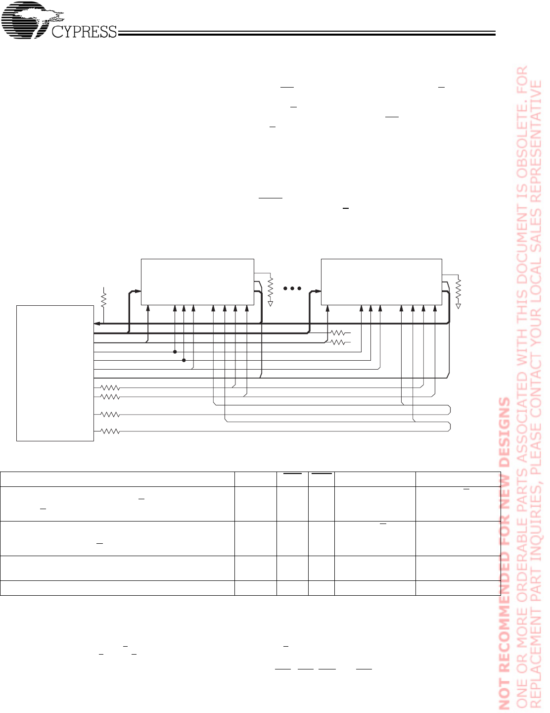
Application Example
[1]
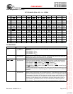
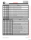
Truth Table
[ 2, 3, 4, 5, 6, 7]
Operation K RPS WPS DQ DQ
Write Cycle:
Load address on the rising edge of K
clock; input write data
on K and K
rising edges.
L-H X L D(A + 0)at K(t) ↑ D(A + 1) at K
(t) ↑
Read Cycle:
Load address on the rising edge of K clock; wait one and a
half cycle; read data on C
and C rising edges.
L-H L X Q(A + 0) at C
(t + 1)↑ Q(A + 1) at C(t + 2) ↑
NOP: No Operation L-H H H D=X
Q=High-Z
D=X
Q=High-Z
Standby: Clock Stopped Stopped X X Previous State Previous State
Notes:
1. The above application shows 4 QDRII being used.
2. X = “Don't Care,” H = Logic HIGH, L= Logic LOW,
↑represents rising edge.
3. Device will power-up deselected and the outputs in a tri-state condition.
4. “A” represents address location latched by the devices when transaction was initiated. A+00, A+01 represents the internal address sequence in the burst.
5. “t” represents the cycle at which a read/write operation is started. t+1 and t+2 are the first and second clock cycles respectively succeeding the “t” clock cycle.
6. Data inputs are registered at K and K
rising edges. Data outputs are delivered on C and C rising edges, except when in single clock mode.
7. It is recommended that K = K
and C = C = HIGH when clock is stopped. This is not essential, but permits most rapid restart by overcoming transmission line
charging symmetrically.
8. Assumes a Write cycle was initiated per the Write Port Cycle Description Truth Table. BWS
0
, BWS
1
, BWS
2
, and BWS
3
can be altered on different portions of a
write cycle, as long as the set-up and hold requirements are achieved.
Vt = Vddq/2
CC#
D
A
K
CC#
D
A
K
BUS
MASTER
(CPU
or
ASIC)
SRAM #1
SRAM #4
DATA IN
DATA OUT
Address
RPS#
WPS#
BWS#
Source K
Source K#
Delayed K
Delayed K#
R = 50ohms
R = 250ohms
R = 250ohms
R
P
S
#
W
P
S
#
B
W
S
#
R
P
S
#
W
P
S
#
B
W
S
#
Vt
Vt
Vt
R
R
R
ZQ
CQ/CQ#
Q
K#
ZQ
CQ/CQ#
Q
K#
CLKIN/CLKIN#
[+] Feedback


