CY7C1310AV18
CY7C1312AV18
CY7C1314AV18
PRELIMINARY
Document #: 38-05497 Rev. *A Page 5 of 21
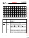
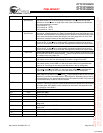
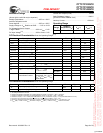
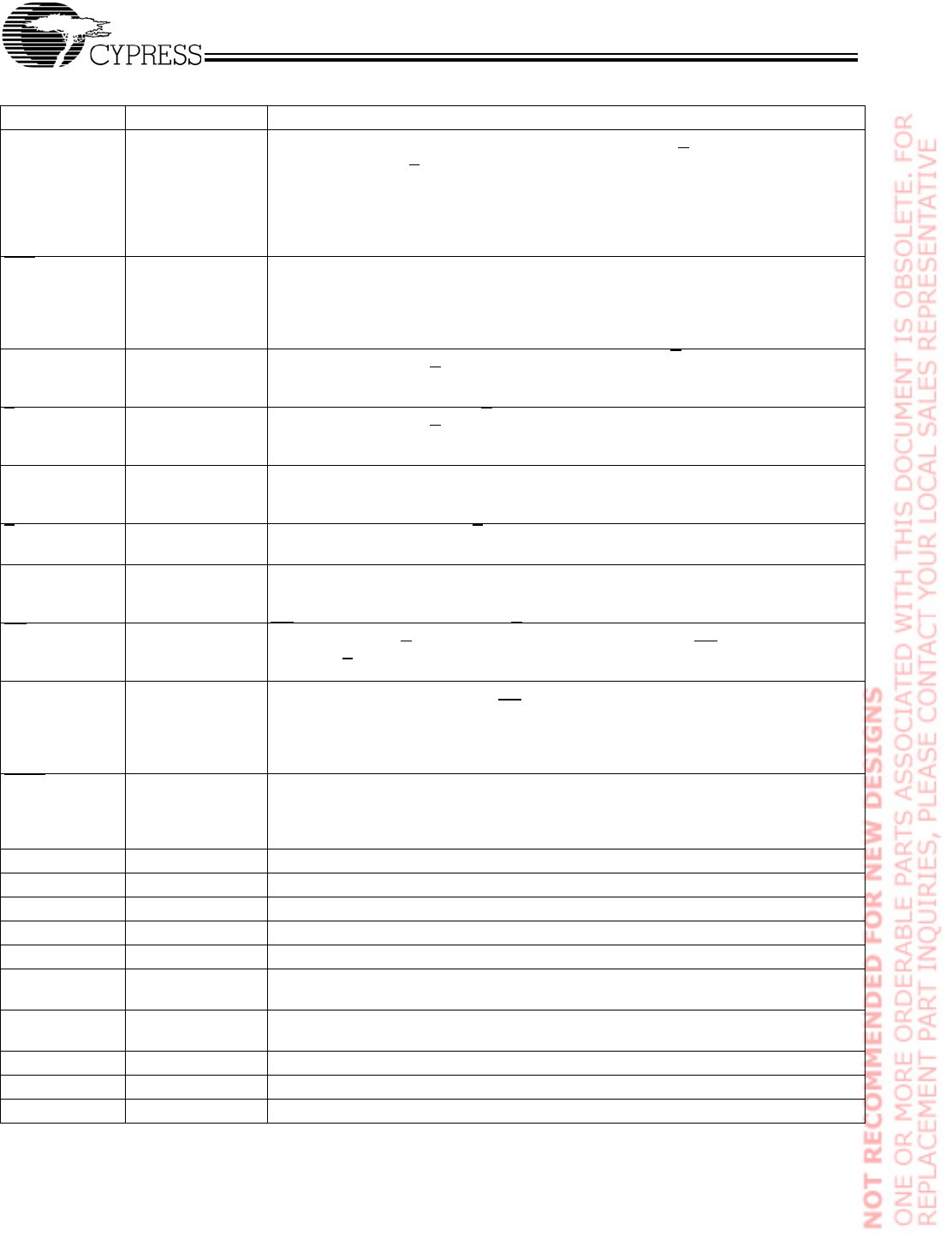
Q
[x:0]
Outputs-
Synchronous
Data Output signals. These pins drive out the requested data during a Read operation.
Valid data is driven out on the rising edge of both the C and C
clocks during Read
operations or K and K
when in single clock mode. When the Read port is deselected,
Q
[x:0]
are automatically tri-stated.
CY7C1310AV18 − Q
[7:0]
CY7C1312AV18 − Q
[17:0]
CY7C1314AV18 − Q
[35:0]
RPS Input-
Synchronous
Read Port Select, active LOW. Sampled on the rising edge of Positive Input Clock (K).
When active, a Read operation is initiated. Deasserting will cause the Read port to be
deselected. When deselected, the pending access is allowed to complete and the output
drivers are automatically tri-stated following the next rising edge of the C clock. Each
read access consists of a burst of two sequential transfers.
C Input-Clock Positive Output Clock Input. C is used in conjunction with C to clock out the Read data
from the device. C and C
can be used together to deskew the flight times of various
devices on the board back to the controller. See application example for further details.
C
Input-Clock Negative Output Clock Input. C is used in conjunction with C to clock out the Read data
from the device. C and C
can be used together to deskew the flight times of various
devices on the board back to the controller. See application example for further details.
K Input-Clock Positive Input Clock Input. The rising edge of K is used to capture synchronous inputs
to the device and to drive out data through Q
[x:0]
when in single clock mode. All accesses
are initiated on the rising edge of K.
K
Input-Clock Negative Input Clock Input. K is used to capture synchronous inputs being presented
to the device and to drive out data through Q
[x:0]
when in single clock mode.
CQ Echo Clock CQ is referenced with respect to C. This is a free running clock and is synchronized
to the output clock(C) of the QDR-II. In the single clock mode, CQ is generated with
respect to K. The timings for the echo clocks are shown in the AC timing table.
CQ
Echo Clock CQ is referenced with respect to C. This is a free running clock and is synchronized
to the output clock(C
) of the QDR-II. In the single clock mode, CQ is generated with
respect to K
. The timings for the echo clocks are shown in the AC timing table.
ZQ Input Output Impedance Matching Input. This input is used to tune the device outputs to the
system data bus impedance. CQ,CQ
and Q
[x:0]
output impedance are set to 0.2 x RQ,
where RQ is a resistor connected between ZQ and ground. Alternately, this pin can be
connected directly to V
DD
, which enables the minimum impedance mode. This pin cannot
be connected directly to GND or left unconnected.
DOFF
Input DLL Turn Off – Active LOW. Connecting this pin to ground will turn off the DLL inside
the device. The timings in the DLL turned off operation will be different from those listed
in this data sheet. More details on this operation can be found in the application note,
“DLL Operation in the QDR-II.”
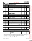
TDO Output TDO for JTAG.
TCK Input TCK pin for JTAG.
TDI Input TDI pin for JTAG.
TMS Input TMS pin for JTAG.
NC N/A Not connected to the die. Can be tied to any voltage level.
NC/36M N/A Address expansion for 36M. This is not connected to the die and so can be tied to any
voltage level.
NC/72M N/A Address expansion for 72M. This is not connected to the die and so can be tied to any
voltage level.
V
SS
/72M Input Address expansion for 72M. This must be tied LOW on the 18M devices.
V
SS
/144M Input Address expansion for 144M. This must be tied LOW on the 18M devices.
V
SS/
288M Input Address expansion for 288M. This must be tied LOW on the 18M devices.
Pin Definitions (continued)
Pin Name I/O Pin Description
[+] Feedback


