PRELIMINARY
CY7C1330AV25
CY7C1332AV25
Document No: 001-07844 Rev. *A Page 4 of 19
Introduction
Functional Overview
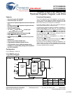
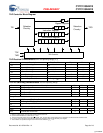
The CY7C1330AV25 and CY7C1332AV25 are synchronous-
pipelined Late Write SRAMs running at speeds up to 250 MHz.
All synchronous inputs pass through input registers controlled
by the rising edge of the clock. All data outputs pass through
output registers controlled by the rising edge of the clock.
Maximum access delay from the clock rise (t
CO
) is 2.0 ns
(250-MHz device).
Accesses can be initiated by asserting Chip Enable (CE
) on
the rising edge of the clock. The address presented to the
device will be latched on this edge of the clock. The access
can either be a read or write operation, depending on the
status of the Write Enable (WE
). BWS
[d:a]
can be used to
conduct individual byte write operations.
Write operations are qualified by the Write Enable (WE
). All
writes are simplified with on-chip synchronous self-timed late
write circuitry.
All operations (Reads, Writes, and Deselects) are pipelined.
Pipelined Read Accesses
A read access is initiated when the following conditions are
satisfied at clock rise: (1) Chip Enable (CE) is asserted active
and (2) the Write Enable input signal (WE)
is asserted HIGH.
The address presented to the address inputs is latched into
the Address Register and presented to the memory core and
control logic. The control logic determines that a read access
is in progress and allows the requested data to propagate to
the input of the output register. At the rising edge of the next
clock the requested data is allowed to propagate through the
output register and onto the data bus within 2.0 ns (250-MHz
device) provided OE
is active LOW. After the first clock of the
read access the output buffers are controlled by OE
and the
internal control logic. OE
must be driven LOW in order for the
device to drive out the requested data. During the second
clock, a subsequent operation (Read/Write/Deselect) can be
initiated. Deselecting the device is also pipelined. Therefore,
when the SRAM is deselected at clock rise by one of the chip
enable signals, its output will tri-state following the next clock
rise.
Bypass Read Operation
Bypass read operation occurs when the last write operation is
followed by a read operation where write and read addresses
are identical. The data outputs are provided from the data in
registers rather than the memory array. This operation occurs
on a byte to byte basis. If only one byte is written during a write
operation and a read operation is performed on the same
address; then a partial bypass read operation is performed
since the new byte data will be from the datain registers while
the remaining bytes are from the memory array.
Late Write Accesses
The Late Write feature allows for the write data to be presented
one cycle later after the access is started. This feature elimi-
nates one bus-turnaround cycle which is necessary when
going from a read to a write in an ordinary pipelined
Synchronous Burst SRAM.
Write access is initiated when the following conditions are
satisfied at clock rise: (1) CE
is asserted active and (2) the
write signal WE
is asserted LOW. The address presented to
A
x
is loaded into the Address Register. The write signals are
latched into the Control Logic block.
The data lines are automatically tri-stated regardless of the
state of the OE
input signal when a write is detected. This
allows the external logic to present the data on DQ
and DQP
(DQ
[a:b]
for CY7C1332AV25 and DQ
[a:d]
for CY7C1330AV25).
In addition, the address for the subsequent access
(Read/Write/Deselect) is latched into the Address Register
(provided the appropriate control signals are asserted).
On the next clock rise the data presented to DQ
(or a subset
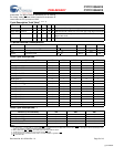
for byte write operations, see Write Cycle Description table for
details) inputs is latched into the device and the write is
complete.
The data written during the Write operation is controlled by
BWS (BWS
[a:d]
for CY7C1330AV25 and BWS
[a:b]
for
CY7C1332AV25) signals. The CY7C1330AV25 and
CY7C1332AV25 provide byte write capability that is described
in the Write Cycle Description table. Asserting the Write
Enable input (WE
) with the selected Byte Write Select (BWS)
input will selectively write to only the desired bytes. Bytes not
selected during a byte write operation will remain unaltered. A
Synchronous self-timed write mechanism has been provided
to simplify the write operations. Byte write capability has been
included in order to greatly simplify Read/Modify/Write
sequences, which can be reduced to simple byte write opera-
tions.
Because the CY7C1330AV25/CY7C1332AV25 is a common
I/O device, data should not be driven into the device while the
outputs are active. The Output Enable (OE
) can be deasserted
HIGH before presenting data to the DQ
inputs. Doing so will
tri-state the output drivers. As a safety precaution, DQ
is
automatically tri-stated during the data portion of a write cycle,
regardless of the state of OE.
Power-up/Power-down Supply Voltage Sequencing
The power-up and power-down supply voltage application
recommendations are as follows:
Power-up: V
SS
, V
DD
, V
DDQ
, V
REF
, V
IN
.
Power-down: V
IN
, V
REF
, V
DDQ
, V
DD
, V
SS
.
V
DDQ
can be applied/removed simultaneously with V
DD
as
long as V
DDQ
does not exceed V
DD
by more than 0.5V.
Programmable Impedance
An external resistor, RQ, must be connected between the ZQ
pin on the SRAM and V
SS
to allow the SRAM to adjust its
output driver impedance. The value of RQ must be 5X the
value of the intended line impedance driven by the SRAM, The
allowable range of RQ to guarantee impedance matching with
a tolerance of ±10% is between 175Ω and 350Ω
, with
V
DDQ
=1.5V. The output impedance is adjusted every 1024
cycles to adjust for drifts in supply voltage and temper-
ature.The output buffers can also be programmed in a
minimum impedance configuration by connecting ZQ to V
DD
.
Sleep Mode
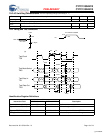
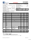
The ZZ input pin is an asynchronous input. Asserting ZZ
places the SRAM in a power conservation “sleep” mode. Two
clock cycles are required to enter into or exit from this “sleep”
mode. While in this mode, data integrity is guaranteed.
Accesses pending when entering the “sleep” mode are not
considered valid nor is the completion of the operation
[+] Feedback


