CY7C1347G
Document #: 38-05516 Rev. *F Page 21 of 22
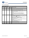
Document History Page
Document Title: CY7C1347G 4-Mbit (128K x 36) Pipelined Sync SRAM
Document Number: 38-05516
REV. ECN
Submission
Date
Orig. of
Change
Description of Change
** 224364 See ECN RKF New data sheet
*A 276690 See ECN VBL Changed TQFP package in Ordering Information section to lead-free TQFP
Added comment of BG and BZ lead-free package availability
*B 333625 See ECN SYT Removed 225 MHz and 100 MHz speed grades
Modified Address Expansion balls in the pinouts for 100 TQFP Package as per
JEDEC standards and updated the Pin Definitions accordingly
Modified V
OL,
V
OH
test conditions
Replaced TBDs for Θ
JA
and Θ
JC
to their respective values on the Thermal Resis-
tance table
Changed the package name for 100 TQFP from A100RA to A101
Removed comment on the availability of BG lead-free package
Updated the Ordering Information by shading and unshading MPNs as per
availability
*C 419256 See ECN RXU Converted from Preliminary to Final.
Changed address of Cypress Semiconductor Corporation on Page #1 from “3901
North First Street” to “198 Champion Court”
Swapped typo CE
2
and
CE
3
in the Truth Table column heading on Page #6
Modified test condition from V
IH
< V
DD
to
V
IH
< V
DD.
Modified test condition from V
DDQ
< V
DD
to V
DDQ
< V
DD
Modified “Input Load” to “Input Leakage Current except ZZ and MODE” in the
Electrical Characteristics Table.
Replaced Package Name column with Package Diagram in the Ordering Infor-
mation table.
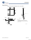
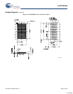
Replaced Package Diagram of 51-85050 from *A to *B
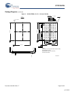
Replaced Package Diagram of 51-85180 from ** to *A
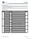
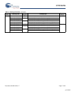
Updated the Ordering Information.
*D 480124 See ECN VKN Added the Maximum Rating for Supply Voltage on V
DDQ
Relative to GND.
Updated the Ordering Information table.
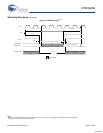
*E 1078184 See ECN VKN Corrected write timing diagram on page 12
*F 2633279 01/15/2009 NXR/AESA Updated Ordering Information and data sheet template.
[+] Feedback


