CY7C1361C
CY7C1363C
Document #: 38-05541 Rev. *F Page 13 of 31
TDI and TDO balls as shown in the Tap Controller Block
Diagram. Upon power-up, the instruction register is loaded
with the IDCODE instruction. It is also loaded with the IDCODE
instruction if the controller is placed in a reset state as
described in the previous section.
When the TAP controller is in the Capture-IR state, the two
least significant bits are loaded with a binary “01” pattern to
allow for fault isolation of the board-level serial test data path.
Bypass Register
To save time when serially shifting data through registers, it is
sometimes advantageous to skip certain chips. The bypass
register is a single-bit register that can be placed between the
TDI and TDO balls. This allows data to be shifted through the
SRAM with minimal delay. The bypass register is set LOW
(V
SS
) when the BYPASS instruction is executed.
Boundary Scan Register
The boundary scan register is connected to all the input and
bidirectional balls on the SRAM.
The boundary scan register is loaded with the contents of the
RAM I/O ring when the TAP controller is in the Capture-DR
state and is then placed between the TDI and TDO balls when
the controller is moved to the Shift-DR state. The EXTEST,
SAMPLE/PRELOAD and SAMPLE Z instructions can be used
to capture the contents of the I/O ring.
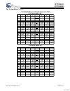
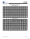
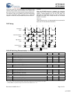
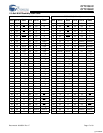
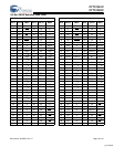
The Boundary Scan Order tables show the order in which the
bits are connected. Each bit corresponds to one of the bumps
on the SRAM package. The MSB of the register is connected
to TDI and the LSB is connected to TDO.
Identification (ID) Register
The ID register is loaded with a vendor-specific, 32-bit code
during the Capture-DR state when the IDCODE command is
loaded in the instruction register. The IDCODE is hardwired
into the SRAM and can be shifted out when the TAP controller
is in the Shift-DR state. The ID register has a vendor code and
other information described in the Identification Register
Definitions table.
TAP Instruction Set
Overview
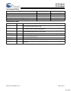
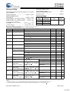
Eight different instructions are possible with the three-bit
instruction register. All combinations are listed in the
Instruction Codes table. Three of these instructions are listed
as RESERVED and should not be used. The other five instruc-
tions are described in detail below.
The TAP controller used in this SRAM is not fully compliant to
the 1149.1 convention because some of the mandatory 1149.1
instructions are not fully implemented.
The TAP controller cannot be used to load address data or
control signals into the SRAM and cannot preload the I/O
buffers. The SRAM does not implement the 1149.1 commands
EXTEST or INTEST or the PRELOAD portion of
SAMPLE/PRELOAD; rather, it performs a capture of the I/O
ring when these instructions are executed.
Instructions are loaded into the TAP controller during the
Shift-IR state when the instruction register is placed between
TDI and TDO. During this state, instructions are shifted
through the instruction register through the TDI and TDO balls.
To execute the instruction once it is shifted in, the TAP
controller needs to be moved into the Update-IR state.
EXTEST
EXTEST is a mandatory 1149.1 instruction which is to be
executed whenever the instruction register is loaded with all
0s. EXTEST is not implemented in this SRAM TAP controller,
and therefore this device is not compliant to 1149.1. The TAP
controller does recognize an all-0 instruction.
When an EXTEST instruction is loaded into the instruction
register, the SRAM responds as if a SAMPLE/PRELOAD
instruction has been loaded. There is one difference between
the two instructions. Unlike the SAMPLE/PRELOAD
instruction, EXTEST places the SRAM outputs in a High-Z
state.
IDCODE
The IDCODE instruction causes a vendor-specific, 32-bit code
to be loaded into the instruction register. It also places the
instruction register between the TDI and TDO balls and allows
the IDCODE to be shifted out of the device when the TAP
controller enters the Shift-DR state.
The IDCODE instruction is loaded into the instruction register
upon power-up or whenever the TAP controller is given a test
logic reset state.
SAMPLE Z
The SAMPLE Z instruction causes the boundary scan register
to be connected between the TDI and TDO balls when the TAP
controller is in a Shift-DR state. It also places all SRAM outputs
into a High-Z state.
SAMPLE/PRELOAD
SAMPLE/PRELOAD is a 1149.1-mandatory instruction. When
the SAMPLE/PRELOAD instructions are loaded into the in-
struction register and the TAP controller is in the Capture-DR
state, a snapshot of data on the inputs and output pins is cap-
tured in the boundary scan register.
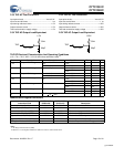
The user must be aware that the TAP controller clock can only
operate at a frequency up to 20 MHz, while the SRAM clock
operates more than an order of magnitude faster. Because
there is a large difference in the clock frequencies, it is possi-
ble that during the Capture-DR state, an input or output will
undergo a transition. The TAP may then try to capture a signal
while in transition (metastable state). This will not harm the
device, but there is no guarantee as to the value that will be
captured. Repeatable results may not be possible.
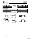
To guarantee that the boundary scan register will capture the
correct value of a signal, the SRAM signal must be stabilized
long enough to meet the TAP controller's capture set-up plus
hold times (t
CS
and t
CH
). The SRAM clock input might not be
captured correctly if there is no way in a design to stop (or
slow) the clock during a SAMPLE/PRELOAD instruction. If this
is an issue, it is still possible to capture all other signals and
simply ignore the value of the CK and CK# captured in the
boundary scan register.
Once the data is captured, it is possible to shift out the data by
putting the TAP into the Shift-DR state. This places the bound-
ary scan register between the TDI and TDO pins.
[+] Feedback


