CY7C138, CY7C139
Document #: 38-06037 Rev. *D Page 9 of 17
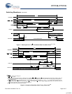
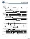
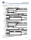
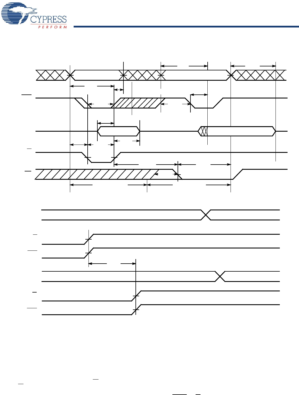
Figure 9. Timing Diagram of Semaphore Contention
[27, 28, 29]
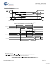
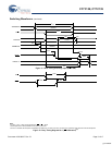
Figure 10. Timing Diagram of Read with BUSY (M/S = HIGH)
[21]
Switching Waveforms (continued)
t
SOP
t
AA
SEM
R/W
OE
I/O
0
VALID ADDRESS VALID ADDRESS
t
HD
DATA
IN
VALID
DATA
OUT
VALID
t
OHA
A
0
–A
2
t
AW
t
HA
t
ACE
t
SOP
t
SCE
t
SD
t
SA
t
PWE
t
SWRD
t
DOE
WRITE CYCLE READ CYCLE
MATCH
t
SPS
A
0L
–A
2L
MATCH
R/W
L
SEM
L
A
0R
–A
2R
R/W
R
SEM
R
Notes
25.Data I/O pins enter high impedance when OE
is held LOW during write.
26.CE
= HIGH for the duration of the above timing (both write and read cycle).
[+] Feedback


