CY7C1440AV33
CY7C1442AV33
CY7C1446AV33
Document #: 38-05383 Rev. *E Page 30 of 31
Document History Page
Document Title: CY7C1440AV33/CY7C1442AV33/CY7C1446AV33 36-Mbit (1M x 36/2M x 18/512K x 72) Pipelined Sync
SRAM
Document Number: 38-05383
REV. ECN NO. Issue Date
Orig. of
Change Description of Change
** 124437 03/04/03 CJM New data sheet
*A 254910 See ECN SYT Part number changed from previous revision. New and old part number differ
by the letter “A”
Modified Functional Block diagrams
Modified switching waveforms
Added Boundary scan information
Added Footnote #14 (32-Bit Vendor ID Code changed)
Added I
DD
, I
X
and I
SB
values in the DC Electrical Characteristics
Added t
POWER
specifications in Switching Characteristics table
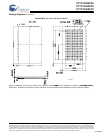
Removed 119 PBGA package
Changed 165 FBGA package from BB165C (15 x 17 x 1.20 mm) to BB165
(15 x 17 x 1.40 mm)
Changed 209-Lead PBGA BG209 (14 x 22 x 2.20 mm) to BB209A (14 x 22
x 1.76 mm)
*B 306335 See ECN SYT Changed H9 pin from V
SSQ
to V
SS
on the Pin Configuration table for 209
FBGA on Page # 6
Changed t
CO
from 3.0 to 3.2 ns and t
DOH
from 1.3 ns to 1.5 ns for 200 Mhz
speed bin on the Switching Characteristics table on Page # 19
Changed Θ
JA
and Θ
JC
from TBD to 25.21 and 2.58 °C/W respectively for
TQFP Package on Pg # 19
Replaced
Θ
JA
and Θ
JC
from TBD to respective Values for 165 BGA and 209
FBGA Packages on the Thermal Resistance Table
Added lead-free information for 100-pin TQFP, 165 FBGA and 209 FBGA
Packages
Changed IDD from 450, 400 and 350 mA to 475, 425 and 375 mA for
frequencies of 250, 200 and 167 MHz respectively
Changed I
SB1 from 190, 180 and 170 mA to 225 mA for frequencies of 250,
200 and 167 MHz respectively
Changed ISB2 from 80 to 100 mA
Changed I
SB3 from 180, 170 and 160 mA to 200 mA for frequencies of 250,
200 and 167 MHz respectively
Changed ISB4 from 100 to 110 mA
*C 332173 See ECN SYT Modified Address Expansion balls in the pinouts for 165 FBGA and 209
FBGA Package as per JEDEC standards
Modified V
OL,
V
OH
test conditions
Changed C
IN
, C
CLK
and C
I/O
to 7, 7and 6 pF from 5, 5 and 7 pF for 165 FBGA
Package
Changed I
SB2
and I
SB4
from 100 and 110 mA to 120 and 135 mA respectively
Added Industrial Temperature Grade
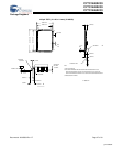
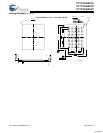
Included the missing 100 TQFP Package Diagram
Updated the Ordering Information by Shading and Unshading MPNs as per
availability
*D 417547 See ECN RXU Converted from Preliminary to Final
Changed address of Cypress Semiconductor Corporation on Page# 1 from
“3901 North First Street” to “198 Champion Court”
Changed I
X
current value in MODE from –5 & 30 µA to –30 & 5 µA respec-
tively and also Changed I
X
current value in ZZ from –30 & 5 µA to –5 & 30
µA respectively on page# 18
Modified test condition in note# 8 from V
IH
< V
DD
to
V
IH
< V
DD
Modified “Input Load” to “Input Leakage Current except ZZ and MODE” in the
Electrical Characteristics Table
Replaced Package Name column with Package Diagram in the Ordering
Information table
Replaced Package Diagram of 51-85050 from *A to *B
Updated the Ordering Information
[+] Feedback


