CY7C64013C
CY7C64113C
Document #: 38-08001 Rev. *B Page 15 of 51
5.2 8-Bit Accumulator (A)
The accumulator is the general-purpose register for the microcontroller.
5.3 8-Bit Temporary Register (X)
The “X” register is available to the firmware for temporary storage of intermediate results. The microcontroller can perform indexed
operations based on the value in X. Refer to Section 5.6.3 for additional information.
5.4 8-Bit Program Stack Pointer (PSP)
During a reset, the program stack pointer (PSP) is set to 0x00 and “grows” upward from this address. The PSP may be set by
firmware, using the MOV PSP,A instruction. The PSP supports interrupt service under hardware control and CALL, RET, and
RETI instructions under firmware control. The PSP is not readable by the firmware.
During an interrupt acknowledge, interrupts are disabled and the 14-bit program counter, carry flag, and zero flag are written as
two bytes of data memory. The first byte is stored in the memory addressed by the PSP, then the PSP is incremented. The second
byte is stored in memory addressed by the PSP, and the PSP is incremented again. The overall effect is to store the program
counter and flags on the program “stack” and increment the PSP by two.
The Return from Interrupt (RETI) instruction decrements the PSP, then restores the second byte from memory addressed by the
PSP. The PSP is decremented again and the first byte is restored from memory addressed by the PSP. After the program counter
and flags have been restored from stack, the interrupts are enabled. The overall effect is to restore the program counter and flags
from the program stack, decrement the PSP by two, and reenable interrupts.
The Call Subroutine (CALL) instruction stores the program counter and flags on the program stack and increments the PSP by
two.
The Return from Subroutine (RET) instruction restores the program counter but not the flags from the program stack and decre-
ments the PSP by two.
5.4.1 Data Memory Organization
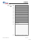
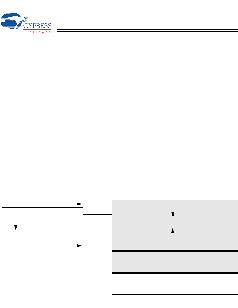
The CY7C64x13C microcontrollers provide 256 bytes of data RAM. Normally, the SRAM is partitioned into four areas: program
stack, user variables, data stack, and USB endpoint FIFOs. The following is one example of where the program stack, data stack,
and user variables areas could be located.
After reset Address
8-bit DSP 8-bit PSP 0x00 Program Stack Growth
(Move DSP
[1]
)
8-bit DSP
user selected Data Stack Growth
User variables
USB FIFO space for five endpoints
[2]
0xFF
Notes:
1. Refer to Section 5.5 for a description of DSP.
2. Endpoint sizes are fixed by the Endpoint Size Bit (I/O register 0x1F, Bit 7), see Table 18-1.
[+] Feedback


