CY7C64013C
CY7C64113C
Document #: 38-08001 Rev. *B Page 24 of 51
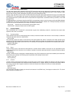
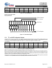
Timer MSB ADDRESS 0x25
Bit [3:0]: Timer higher nibble
Bit [7:4]: Reserved
12.0 I
2
C and HAPI Configuration Register
Internal hardware supports communication with external devices through two interfaces: a two-wire I
2
C-compatible interface, and
a HAPI for 1, 2, or 3 byte transfers. The I
2
C-compatible interface and HAPI functions, discussed in detail in Sections 13.0 and
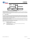
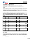
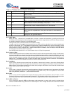
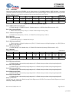
14.0, share a common configuration register (see Figure 12-1). All bits of this register are cleared on reset.
I
2
C Configuration ADDRESS 0x09
Note: I
2
C-compatible function must be separately enabled as described in Section 13.0.
Bits [7,1:0] of the HAPI/I
2
C Configuration Register control the pin out configuration of the HAPI and I
2
C-compatible interfaces.
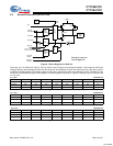
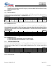
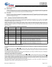
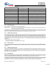
Bits [5:2] are used in HAPI mode only, and are described in Section 14.0. Table 12-1 shows the HAPI port configurations, and
Table 12-2 shows I
2
C pin location configuration options. These I
2
C-compatible options exist due to pin limitations in certain
packages, and to allow simultaneous HAPI and I
2
C-compatible operation.
HAPI operation is enabled whenever either HAPI Port Width Bit (Bit 1 or 0) is non-zero. This affects GPIO operation as described
in Section 14.0. I
2
C-compatible blocks must be separately enabled as described in Section 13.0.
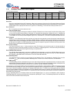
Bit # 76543210
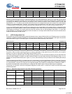
Bit Name Reserved Reserved Reserved Reserved Timer Bit 11 Timer Bit 10 Timer Bit 9 Timer Bit 8
Read/Write ----RRRR
Reset 00000000
Figure 11-2. Timer MSB Register
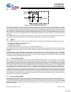
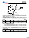
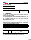
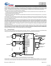
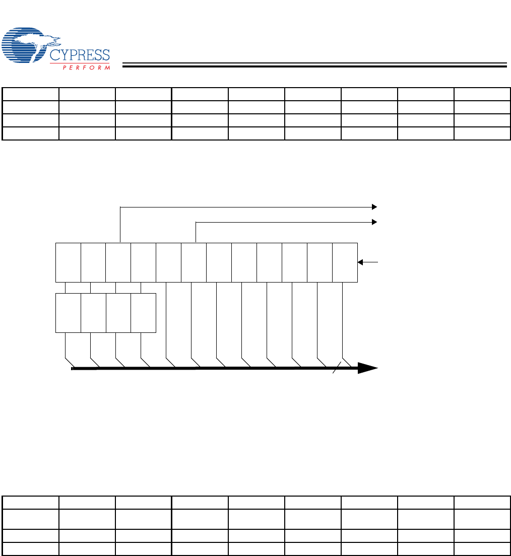
Figure 11-3. Timer Block Diagram
Bit # 76543210
Bit Name I
2
C Position Reserved LEMPTY
Polarity
DRDY
Polarity
Latch
Empty
Data
Ready
HAPI Port Width
Bit 1
HAPI Port Width
Bit 0
Read/Write R/W - R/W R/W R R R/W R/W
Reset 00000000
Figure 12-1. HAPI/I
2
C Configuration Register
10 9 78
5
6432
1-MHz Clock
1.024-ms Interrupt
128-
µs Interrupt
To Timer Register
8
1 011
L1 L0L2L3
D3 D2 D1 D0 D7 D6 D5 D4 D3 D2 D1 D0
[+] Feedback


