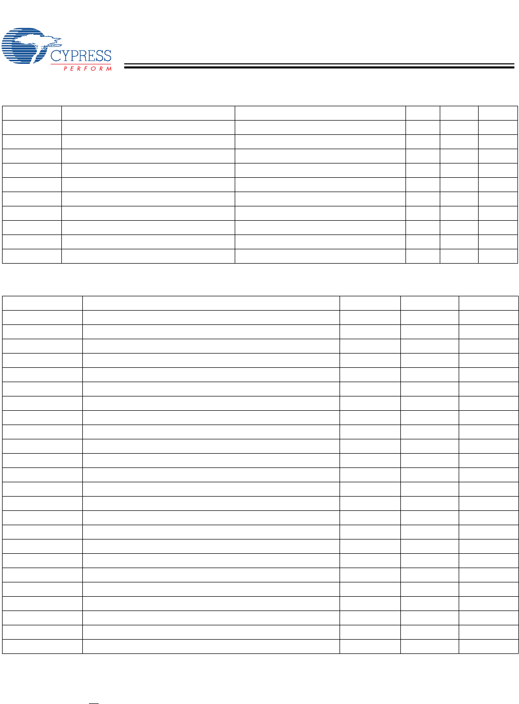
CY7C64013C
CY7C64113C
Document #: 38-08001 Rev. *B Page 46 of 51
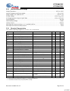
DAC Interface
R
up
DAC Pull-up Resistance (typical 14 kΩ) 8.0 24.0 kΩ
I
sink0(0)
DAC[7:2] Sink current (0) V
out
= 2.0V DC 0.1 0.3 mA
I
sink0(F)
DAC[7:2] Sink current (F) V
out
= 2.0V DC 0.5 1.5 mA
I
sink1(0)
DAC[1:0] Sink current (0) V
out
= 2.0V DC 1.6 4.8 mA
I
sink1(F)
DAC[1:0] Sink current (F) V
out
= 2.0V DC 8 24 mA
I
range
Programmed Isink Ratio: max/min V
out
= 2.0V DC
[6]
46
T
ratio
Tracking Ratio DAC[1:0] to DAC[7:2] V
out
= 2.0V
[7]
14 22
I
sinkDAC
DAC Sink Current V
out
= 2.0V DC 1.6 4.8 mA
I
lin
Differential Nonlinearity DAC Port
[8]
0.6 LSB
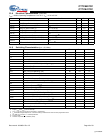
24.0 Switching Characteristics (f
OSC
= 6.0 MHz)
Parameter Description Min. Max. Unit
Clock Source
f
OSC
Clock Rate 6 ±0.25% MHz
t
cyc
Clock Period 166.25 167.08 ns
t
CH
Clock HIGH time 0.45 t
CYC
ns
t
CL
Clock LOW time 0.45 t
CYC
ns
USB Full Speed Signaling
[9]
t
rfs
Transition Rise Time 4 20 ns
t
ffs
Transition Fall Time 4 20 ns
t
rfmfs
Rise / Fall Time Matching; (t
r
/t
f
) 90 111 %
t
dratefs
Full Speed Date Rate 12 ±0.25% Mb/s
DAC Interface
t
sink
Current Sink Response Time 0.8 µs
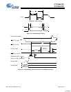
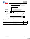
HAPI Read Cycle Timing
t
RD
Read Pulse Width 15 ns
t
OED
OE LOW to Data Valid
[10, 11]
40 ns
t
OEZ
OE HIGH to Data High-Z
[11]
20 ns
t
OEDR
OE LOW to Data_Ready Deasserted
[10, 11]
060ns
HAPI Write Cycle Timing
t
WR
Write Strobe Width 15 ns
t
DSTB
Data Valid to STB HIGH (Data Set-up Time)
[11]
5ns
t
STBZ
STB HIGH to Data High-Z (Data Hold Time)
[11]
15 ns
t
STBLE
STB LOW to Latch_Empty Deasserted
[10, 11]
050ns
Timer Signals
t
watch
Watchdog Timer Period 8.192 14.336 ms
Notes:
6. Irange: I
sinkn
(15)/ I
sinkn
(0) for the same pin.
7. T
ratio
= I
sink1
[1:0](n)/I
sink0
[7:2](n) for the same n, programmed.
8. I
lin
measured as largest step size vs. nominal according to measured full scale and zero programmed values.
9. Per Table 7-6 of revision 1.1 of USB specification.
10. For 25-pF load.
11. Assumes chip select CS
is asserted (LOW).
23.0 Electrical Characteristics (continued)
f
OSC
= 6 MHz; Operating Temperature = 0 to 70°C, V
CC
= 4.0V to 5.25V
Parameter Description Conditions Min. Max. Unit
[+] Feedback


