CY7C6431x
CY7C64345, CY7C6435x
Document Number: 001-12394 Rev *G Page 16 of 28
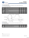
DC General Purpose IO Specifications
Table 11 lists guaranteed maximum and minimum specifications for the voltage and temperature ranges: 3.0V to 5.5V and 0°C ≤ T
A
≤ 70°C. Typical parameters apply to 5V and 3.3V at 25°C. These are for design guidance only.
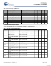
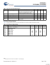
Table 10.DC Characteristics – USB Interface
Symbol Description Conditions Min Typ Max Units
Rusbi USB D+ Pull Up Resistance With idle bus 0.900 - 1.575 kΩ
Rusba USB D+ Pull Up Resistance While receiving traffic 1.425 - 3.090 kΩ
Vohusb Static Output High 2.8 - 3.6 V
Volusb Static Output Low -0.3V
Vdi Differential Input Sensitivity 0.2 - V
Vcm Differential Input Common Mode Range 0.8 - 2.5 V
Vse Single Ended Receiver Threshold 0.8 - 2.0 V
Cin Transceiver Capacitance - 50 pF
Iio High Z State Data Line Leakage On D+ or D- line -10 - +10 μA
Rps2 PS/2 Pull Up Resistance 3 5 7 kΩ
Rext External USB Series Resistor In series with each USB pin 21.76 24.0 24.24 Ω
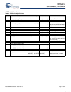
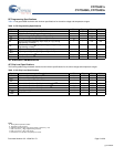
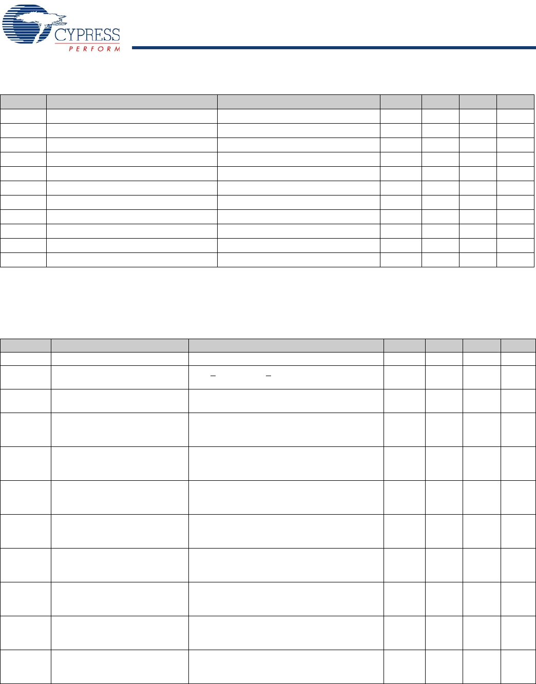
Table 11. 3.0V and 5.5V DC GPIO Specifications
Symbol Description Conditions Min Typ Max Units
R
PU
Pull Up Resistor 4 5.6 8 kΩ
V
OH1
High Output Voltage
Port 0, 2, or 3 Pins
IOH < 10 µA, Vdd > 3.0V, maximum of 10 mA
source current in all I/Os.
Vdd - 0.2 – – V
V
OH2
High Output Voltage
Port 0, 2, or 3 Pins
IOH = 1 mA Vdd > 3.0, maximum of 20 mA
source current in all I/Os.
Vdd - 0.9 – – V
V
OH3
High Output Voltage
Port 1 Pins with LDO Regulator
Disabled
IOH < 10 µA, Vdd > 3.0V, maximum of 10 mA
source current in all I/Os.
Vdd - 0.2 – – V
V
OH4
High Output Voltage
Port 1 Pins with LDO Regulator
Disabled
IOH = 5 mA, Vdd > 3.0V, maximum of 20 mA
source current in all I/Os.
Vdd - 0.9 – – V
V
OH5
High Output Voltage
Port 1 Pins with LDO Regulator
Enabled for 3V Out
IOH < 10 μA, Vdd > 3.1V, maximum of 4 I/Os
all sourcing 5 mA
2.85 3.00 3.3 V
V
OH6
High Output Voltage
Port 1 Pins with LDO Regulator
Enabled for 3V Out
IOH = 5 mA, Vdd > 3.1V, maximum of 20 mA
source current in all I/Os
2.20 – – V
V
OH7
High Output Voltage
Port 1 Pins with LDO Enabled for
2.5V Out
IOH < 10 μA, Vdd > 3.0V, maximum of 20 mA
source current in all I/Os
2.35 2.50 2.75 V
V
OH8
High Output Voltage
Port 1 Pins with LDO Enabled for
2.5V Out
IOH = 2 mA, Vdd > 3.0V, maximum of 20 mA
source current in all I/Os
1.90 – – V
V
OH9
High Output Voltage
Port 1 Pins with LDO Enabled for
1.8V Out
IOH < 10 μA, Vdd > 3.0V, maximum of 20 mA
source current in all I/Os
1.60 1.80 2.1 V
V
OH10
High Output Voltage
Port 1 Pins with LDO Enabled for
1.8V Out
IOH = 1 mA, Vdd > 3.0V, maximum of 20 mA
source current in all I/Os
1.20 – – V
[+] Feedback


