CY7C6431x
CY7C64345, CY7C6435x
Document Number: 001-12394 Rev *G Page 18 of 28
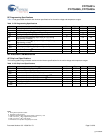
DC Programming Specifications
Table 13 lists guaranteed maximum and minimum specifications for the entire voltage and temperature ranges.
AC Electrical Characteristics
AC Chip Level Specifications
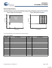
The following tables list guaranteed maximum and minimum specifications for the entire voltage and temperature ranges.
Table 13. DC Programming Specifications
Symbol Description Min Typ Max Units
Vdd
IWRITE
Supply Voltage for Flash Write Operations 3.0 – – V
I
DDP
Supply Current During Programming or Verify – 5 25 mA
V
ILP
Input Low Voltage During Programming or Verify – – V
IL
V
V
IHP
Input High Voltage During Programming or Verify V
IH
– – V
I
ILP
Input Current when Applying Vilp to P1[0] or P1[1] During
Programming or Verify
(8)
– – 0.2 mA
I
IHP
Input Current when Applying Vihp to P1[0] or P1[1] During
Programming or Verify
(8)
– – 1.5 mA
V
OLV
Output Low Voltage During Programming or Verify – – Vss + 0.75 V
V
OHV
Output High Voltage During Programming or Verify Vdd - 0.9 – Vdd V
Flash
ENPB
Flash Write Endurance
(9)
50,000 – – Cycles
Flash
DR
Flash Data Retention
(10)
10 20 – Years
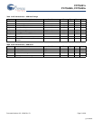
Table 14. AC Chip Level Specifications
Symbol Description Min Typ Max Units
F
MAX
Maximum Operating Frequency
(11)
24 – – MHz
F
CPU
Maximum Processing Frequency
(12)
24 – – MHz
F
32K1
Internal Low Speed Oscillator Frequency 19 32 50 kHz
F
IMO24
Internal Main Oscillator Stability for 24 MHz ± 5%
(13)
22.8 24 25.2 MHz
F
IMO12
Internal Main Oscillator Stability for 12 MHz
(13)
11.4 12 12.6 MHz
F
IMO6
Internal Main Oscillator Stability for 6 MHz
(13)
5.7 6.0 6.3 MHz
DC
IMO
Duty Cycle of IMO 40 50 60 %
T
RAMP
Supply Ramp Time 0 – – μs
Notes
8. Driving internal pull down resistor.
9. Erase/write cycles per block.
10.Following maximum Flash write cycles at Tamb = 55C and Tj = 70C
11. Vdd = 3.0V and T
J
= 85
o
C, digital clocking functions.
12.Vdd = 3.0V and T
J
= 85
o
C, CPU speed.
13.Trimmed for 3.3V operation using factory trim values.
[+] Feedback


