CY7C6431x
CY7C64345, CY7C6435x
Document Number: 001-12394 Rev *G Page 21 of 28
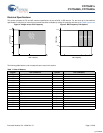
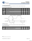
AC Programming Specifications
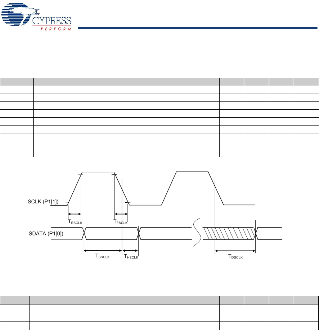
Table 19 lists guaranteed maximum and minimum specifications for the entire voltage and temperature ranges.
Figure 7. Timing Diagram - AC Programming Cycle
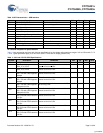
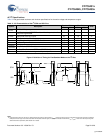
AC SPI Specifications
Table 20 lists guaranteed maximum and minimum specifications for the entire voltage and temperature ranges.
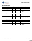
Table 19. AC Programming Specifications
Symbol Description Min Typ Max Units
T
RSCLK
Rise Time of SCLK 1 – 20 ns
T
FSCLK
Fall Time of SCLK 1 – 20 ns
T
SSCLK
Data Setup Time to Falling Edge of SCLK 40 – – ns
T
HSCLK
Data Hold Time from Falling Edge of SCLK 40 – – ns
F
SCLK
Frequency of SCLK 0 – 8 MHz
T
ERASEB
Flash Erase Time (Block) – – 18 ms
T
WRITE
Flash Block Write Time – – 25 ms
T
DSCLK1
Data Out Delay from Falling Edge of SCLK, Vdd > 3.6V – – 60 ns
T
DSCLK2
Data Out Delay from Falling Edge of SCLK, 3.0V<Vdd<3.6V – – 85 ns
Table 20. AC SPI Specifications
Symbol Description Min Typ Max Units
F
SPIM
Maximum Input Clock Frequency Selection, Master
(14)
– – 12 MHz
F
SPIS
Maximum Input Clock Frequency Selection, Slave – – 12 MHz
T
SS
Width of SS_ Negated Between Transmissions 50 – – ns
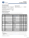
Notes
14.Output clock frequency is half of input clock rate.
[+] Feedback


