CY8C20x36/46/66, CY8C20396
Document Number: 001-12696 Rev. *D Page 23 of 34
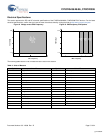
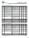
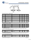
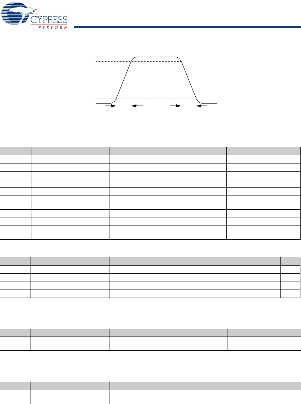
Figure 11. GPIO Timing Diagram
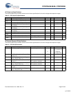
AC Comparator Specifications
The following table lists guaranteed maximum and minimum specifications for the entire voltage and temperature ranges.
AC Analog Mux Bus Specifications
The following table lists guaranteed maximum and minimum specifications for the entire voltage and temperature ranges.
TFall
TRise23
TRise01
90%
10%
GPIO Pin
Output
Voltage
TRise23L
TRise01L
TFallL
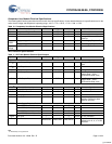
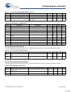
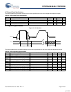
Table 25.AC Characteristics – USB Data Timings
Symbol Description Conditions Min Typ Max Units
Tdrate Full speed data rate Average bit rate 12–0.25% 12 12 + 0.25% MHz
Tdjr1 Receiver data jitter tolerance To next transition -18.5 – 18.5 ns
Tdjr2 Receiver data jitter tolerance To pair transition -9 – 9 ns
Tudj1 Driver differential jitter To next transition -3.5 – 3.5 ns
Tudj2 Driver differential jitter To pair transition -4.0 – 4.0 ns
Tfdeop Source jitter for differential
transition
To SE0 transition -2 – 5 ns
Tfeopt Source SE0 interval of EOP 160 – 175 ns
Tfeopr Receiver SE0 interval of EOP 82 – ns
Tfst Width of SE0 interval during
differential transition
–14ns
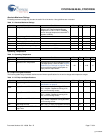
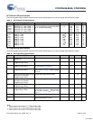
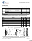
Table 26.AC Characteristics – USB Driver
Symbol Description Conditions Min Typ Max Units
Tr Transition rise time 50 pF 4 – 20 ns
Tf Transition fall time 50 pF 4 – 20 ns
TR Rise/fall time matching 90.00 – 111.1 %
Vcrs Output signal crossover voltage 1.3 – 2.0 V
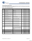
Table 27. AC Low Power Comparator Specifications
Symbol Description Conditions Min Typ Max Units
T
LPC
Comparator Response Time, 50
mV Overdrive
50 mV overdrive does not include
offset voltage.
100 ns
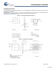
Table 28. AC Analog Mux Bus Specifications
Symbol Description Conditions Min Typ Max Units
F
SW
Switch Rate Maximum pin voltage when measuring
switch rate is 1.8Vp-p
––6.3MHz
[+] Feedback


