CY8C22113, CY8C22213
Document Number: 38-12009 Rev. *F Page 9 of 36
32-Pin Part Pinout
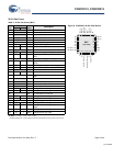
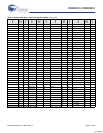
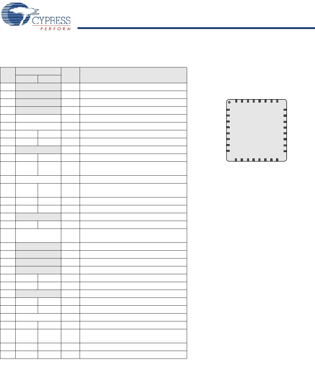
Table 5. 32-Pin Part Pinout (MLF*)
Pin
No.
Type
Pin
Name
Description
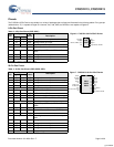
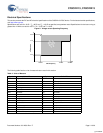
Figure 8. CY8C22213 32-Pin PSoC Device
Digital Analog
1 NC No connection. Do not use.
2 NC No connection. Do not use.
3 NC No connection. Do not use.
4 NC No connection. Do not use.
5 Power Vss Ground connection
6 Power Vss Ground connection
7 IO P1[7] I2C Serial Clock (SCL)
8 IO P1[5] I2C Serial Data (SDA)
9 NC No connection. Do not use.
10 IO P1[3]
11 IO P1[1] Crystal Input (XTALin), I2C Serial Clock
(SCL)
12 Power Vss Ground connection
13 IO P1[0] Crystal Output (XTALout), I2C Serial Data
(SDA)
14 IO P1[2]
15 IO P1[4] Optional External Clock Input (EXTCLK)
16 NC No connection. Do not use.
17 IO P1[6]
18 Input XRES Active high external reset with internal pull
down
19 NC No connection. Do not use.
20 NC No connection. Do not use.
21 NC No connection. Do not use.
22 NC No connection. Do not use.
23 IO I P0[0] Analog column mux input
24 IO I P0[2] Analog column mux input
25 NC No connection. Do not use.
26 IO I P0[4] Analog column mux input
27 IO I P0[6] Analog column mux input
28 Power Vdd Supply voltage
29 IO I P0[7] Analog column mux input
30 IO IO P0[5] Analog column mux input and column
output
31 IO I P0[3] Analog column mux input
32 IO I P0[1] Analog column mux input
LEGEND: A = Analog, I = Input, and O = Output.
* The MLF package has a center pad that must be connected to the same ground as the Vss pin.
NC
NC
NC
NC
Vss
Vss
MLF
(Top View)
9
10
11
12
13
14
15
16
1
2
3
4
5
6
7
8
24
23
22
21
20
19
18
17
32
31
30
29
28
27
26
25
P0[1], AI
P0[3], AI
P0[5], AIO
P0[7], AI
Vdd
P0[6], AI
P0[4], AI
NC
I2C SCL, P1[7]
I2C SDA, P1[5]
P0[2], AI
P0[0], AI
XRES
P1[6]
NC
P1[3]
I2C SCL, XTALin, P1[1]
Vss
I2C SDA, XTALout, P1[0]
P1[2]
EXTCLK, P1[4]
NC
NC
NC
NC
NC
[+] Feedback


