CY8C23433, CY8C23533
Document Number: 001-44369 Rev. *B Page 24 of 37
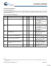
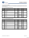
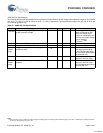
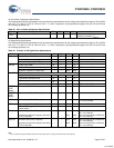
SAR8 ADC DC Specifications
The following table lists the guaranteed maximum and minimum specifications for the voltage and temperature ranges: 4.75V to 5.25V
and -40°C ≤ T
A
≤ 85°C, or 3.0V to 3.6V and -40°C ≤ T
A
≤ 85°C, respectively. Typical parameters apply to 5V and 3.3V at 25°C and
are for design guidance only.
Table 23. SAR8 ADC DC Specifications
Symbol Description Min Typ Max Units Notes
V
ADCVREF
Reference voltage at pin P3[0] when configured
as ADC reference voltage
3.0 – 5.25 V The voltage level at P3[0]
(when configured as ADC
reference voltage) must
always be maintained to be
less than chip supply voltage
level on Vdd pin.
V
ADCVREF
< Vdd.
I
ADCVREF
Current when P3[0] is configured as ADC V
REF
3 ––mA
INL Integral Non-linearity -1.5
–+1.5LSB
INL
(limited
range)
Integral Non-linearity accommodating a shift in
the offset at 0x80
-1.2
[12]
– +1.2 LSB The maximum LSB is over a
sub-range not exceeding
1/16 of the full-scale range.
0x7F and 0x80 points specs
are excluded here
DNL Differential Non-linearity -2.3
– +2.3 LSB ADC conversion is
monotonic over full range
DNL
(limited
range)
Differential Non-linearity excluding 0x7F-0x80
transition
-1
– +1 LSB ADC conversion is
monotonic over full range.
0x7F to 0x80 transition specs
are excluded here.
Notes
12.SAR converters require a stable input voltage during the sampling period. If the voltage into the SAR8 changes by more than 1 LSB during the sampling period then
the accuracy specifications may not be met
[+] Feedback


