


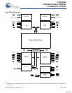
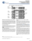
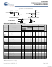
CYD01S36V
CYD02S36V/36VA/CYD04S36V
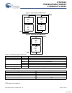
CYD09S36V/CYD18S36V
Document Number: 38-06076 Rev. *G Page 4 of 28
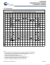
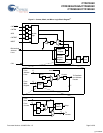
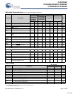
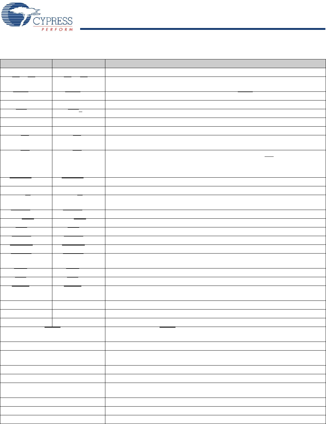
Pin Definitions
Left Port Right Port Description
A
0L
–A
18L
A
0R
–A
18R
Address Inputs.
BE
0L
–BE
3L
BE
0R
–BE
3R
Byte Enable Inputs. Asserting these signals enables Read and Write operations to the
corresponding bytes of the memory array.
BUSY
L
[2,5]
BUSY
R
[2,5]
Port Busy Output. When the collision is detected, a BUSY is asserted.
C
L
C
R
Input Clock Signal.
CE0
L
[11]
CE0
R
[11]
Active Low Chip Enable Input.
CE1
L
[10]
CE1
R
[10]
Active High Chip Enable Input.
DQ
0L
–DQ
35L
DQ
0R
–DQ
35R
Data Bus Input/Output.
OE
L
OE
R
Output Enable Input. This asynchronous signal must be asserted LOW to enable the DQ
data pins during Read operations.
INT
L
INT
R
Mailbox Interrupt Flag Output. The mailbox permits communications between ports. The
upper two memory locations can be used for message passing. INT
L
is asserted LOW
when the right port writes to the mailbox location of the left port, and vice versa. An interrupt
to a port is deasserted HIGH when it reads the contents of its mailbox.
LowSPD
L
[2,4]
LowSPD
R
[2,4]
Port Low Speed Select Input.
PORTSTD[1:0]
L
[2,4]
PORTSTD[1:0]
R
[2,4]
Port Address/Control/Data IO Standard Select Inputs.
R/W
L
R/W
R
Read/Write Enable Input. Assert this pin LOW to write to, or HIGH to Read from the dual
port memory array.
READY
L
[2,5]
READY
R
[2,5]
Port Ready Output. This signal is asserted when a port is ready for normal operation.
CNT/MSK
L
[10]
CNT/MSK
R
[10]
Port Counter/Mask Select Input. Counter control input.
ADS
L
[11]
ADS
R
[11]
Port Counter Address Load Strobe Input. Counter control input.
CNTEN
L
[11]
CNTEN
R
[11]
Port Counter Enable Input. Counter control input.
CNTRST
L
[10]
CNTRST
R
[10]
Port Counter Reset Input. Counter control input.
CNTINT
L
[12]
CNTINT
R
[12]
Port Counter Interrupt Output. This pin is asserted LOW when the unmasked portion of
the counter is incremented to all “1s”.
WRP
L
[2,3]
WRP
R
[2,3]
Port Counter Wrap Input. The burst counter wrap control input.
RET
L
[2,3]
RET
R
[2,3]
Port Counter Retransmit Input. Counter control input.
FTSEL
L
[2,3]
FTSEL
R
[2,3]
Flow-Through Select. Use this pin to select Flow-Through mode. When is de-asserted,
the device is in pipelined mode.
VREF
L
[2,4]
VREF
R
[2,4]
Port External High-Speed IO Reference Input.
V
DDIOL
V
DDIOR
Port IO Power Supply.
REV
L
[2, 3, 4]
REV
R
[2, 3, 4]
Reserved pins for future features.
MRST
Master Reset Input. MRST is an asynchronous input signal and affects both ports. A
maser reset operation is required at power up.
TRST
[2,5]
JTAG Reset Input.
TMS JTAG Test Mode Select Input. It controls the advance of JTAG TAP state machine. State
machine transitions occur on the rising edge of TCK.
TDI JTAG Test Data Input. Data on the TDI input is shifted serially into selected registers.
TCK JTAG Test Clock Input.
TDO JTAG Test Data Output. TDO transitions occur on the falling edge of TCK. TDO is
normally three-stated except when captured data is shifted out of the JTAG TAP.
V
SS
Ground Inputs.
V
CORE
[13]
Core Power Supply.
V
TTL
LVTTL Power Supply for JTAG IOs
[+] Feedback