


CYD01S36V
CYD02S36V/36VA/CYD04S36V
CYD09S36V/CYD18S36V
Document Number: 38-06076 Rev. *G Page 5 of 28
Master Reset
The FLEx36 family devices undergo a complete reset by taking
its MRST
input LOW. The MRST input can switch asynchro-
nously to the clocks. An MRST initializes the internal burst
counters to zero, and the counter mask registers to all ones
(completely unmasked). MRST also forces the Mailbox Interrupt
(INT
) flags and the Counter Interrupt (CNTINT) flags HIGH.
MRST
must be performed on the FLEx36 family devices after
power up.
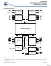
Mailbox Interrupts
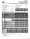
The upper two memory locations may be used for message
passing and permit communications between ports. Table 2
shows the interrupt operation for both ports of CYD18S36V. The
highest memory location, 7FFFF is the mailbox for the right port
and 7FFFE is the mailbox for the left port. Table 2 shows that to
set the INT
R
flag, a Write operation by the left port to address
7FFFF asserts INT
R
LOW. At least one byte must be active for a
Write to generate an interrupt. A valid Read of the 7FFFF
location by the right port resets INT
R
HIGH. At least one byte
must be active in order for a Read to reset the interrupt. When
one port Writes to the other port’s mailbox, the INT of the port
that the mailbox belongs to is asserted LOW. The INT
is reset
when the owner (port) of the mailbox Reads the contents of the
mailbox. The interrupt flag is set in a flow-thru mode (i.e., it
follows the clock edge of the writing port). Also, the flag is reset
in a flow-thru mode (i.e., it follows the clock edge of the reading
port).
Each port can read the other port’s mailbox without resetting the
interrupt. And each port can write to its own mailbox without
setting the interrupt. If an application does not require message
passing, INT
pins must be left open.
Address Counter and Mask Register
Operations
[19]
This section describes the features only apply to 1Mbit, 2 Mbit,
4 Mbit and 9 Mbit devices. It does not apply to 18Mbit device.
Each port of these devices has a programmable burst address
counter. The burst counter contains three registers: a counter
register, a mask register, and a mirror register.
The counter register contains the address used to access the
RAM array. It is changed only by the Counter Load, Increment,
Counter Reset, and by master reset (MRST
) operations.
The mask register value affects the Increment and Counter
Reset operations by preventing the corresponding bits of the
counter register from changing. It also affects the counter
interrupt output (CNTINT
). The mask register is changed only by
the Mask Load and Mask Reset operations, and by the MRST
.
The mask register defines the counting range of the counter
register. It divides the counter register into two regions: zero or
more “0s” in the most significant bits define the masked region,
one or more “1s” in the least significant bits define the unmasked
region. Bit 0 may also be “0,” masking the least significant
counter bit and causing the counter to increment by two instead
of one.l
The mirror register is used to reload the counter register on
increment operations (see “retransmit,” below). It always
contains the value last loaded into the counter register, and is
changed only by the Counter Load, and Counter Reset opera-
tions, and by the MRST
.
Table 3 on page 6 summarizes the operation of these registers
and the required input control signals. The MRST
control signal
is asynchronous. All the other control signals in Table 3 on page
6 (CNT/MSK, CNTRST, ADS, CNTEN) are synchronized to the
port’s CLK. All these counter and mask operations are
independent of the port’s chip enable inputs (CE0 and CE1).
Notes
13.This family of Dual-Ports does not use V
CORE
, and these pins are internally NC. The next generation Dual-Port family, the FLEx36-E™, uses V
CORE
of 1.5V or 1.8V.
Please contact local Cypress FAE for more information.
14.CE
is internal signal. CE = LOW if CE
0
= LOW and CE
1
= HIGH. For a single Read operation, CE only needs to be asserted once at the rising edge of the CLK and
can be deasserted after that. Data is out after the following CLK edge and is three-stated after the next CLK edge.
15.OE
is “Don’t Care” for mailbox operation.
16.At least one of BE0
, BE1, BE2, or BE3 must be LOW.
17. A17x is a NC for CYD04S36V, therefore the Interrupt Addresses are 1FFFF and 1FFFE. A17x and A16x are NC for CYD02S36V/36VA, therefore the Interrupt Addresses
are FFFF and FFFE; A17x, A16x and A15x are NC for CYD01S36V, therefore the Interrupt Addresses are 7FFF and 7FFE.
18.“X” = “Don’t Care,” “H” = HIGH, “L” = LOW.
19.This section describes the CYD09S36V, CYD04S36V, CYD02S36V/36VA, and CYD01S36V which have 18, 17, 16 and 15 address bits.
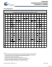
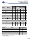
Table 2. Interrupt Operation Example
[1, 14, 15, 16, 17, 18]
Function
Left Port Right Port
R/W
L
CE
L
A
0L–18L
INT
L
R/W
R
CE
R
A
0R–18R
INT
R
Set Right INT
R
Flag L L 7FFFF X X X X L
Reset Right INT
R
FlagXXXXHL7FFFFH
Set Left INT
L
Flag X X X L L L 7FFFE X
Reset Left INT
L
Flag H L 7FFFE H X X X X
[+] Feedback