


CYDC256B16, CYDC128B16,
CYDC064B16, CYDC128B08,
CYDC064B08
Document #: 001-01638 Rev. *E Page 18 of 26
Switching Waveforms
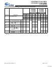
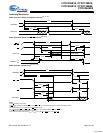
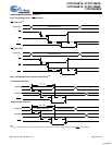
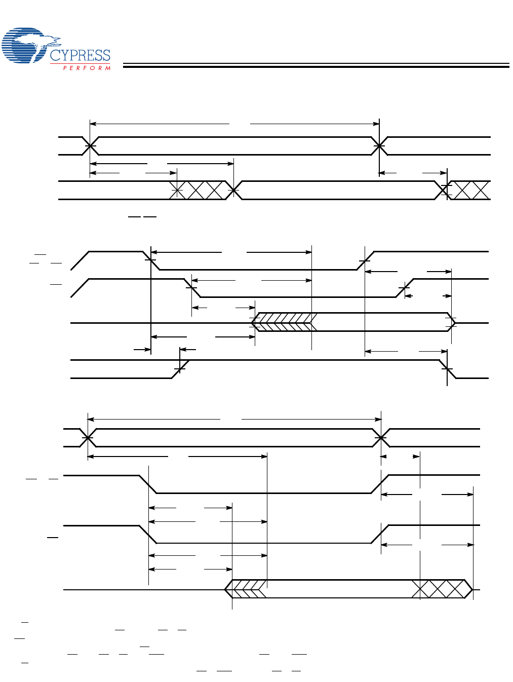
Read Cycle No.1 (Either Port Address Access)
[36, 37, 38]
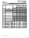
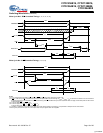
Read Cycle No.2 (Either Port CE/OE Access)
[36, 39, 40]
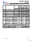
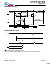
Read Cycle No. 3 (Either Port)
[36, 38, 41, 42]
Notes:
36.R/W
is HIGH for read cycles.
37.Device is continuously selected CE
= V
IL
and UB or LB = V
IL
. This waveform cannot be used for semaphore reads.
38.OE
= V
IL
.
39.Address valid prior to or coincident with CE
transition LOW.
40.To access RAM, CE
= V
IL
, UB or LB = V
IL
, SEM = V
IH
. To access semaphore, CE = V
IH
, SEM = V
IL
.
41.R/W
must be HIGH during all address transitions.
42.A write occurs during the overlap (t
SCE
or t
PWE
) of a LOW CE or SEM and a LOW UB or LB.
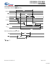
t
RC
t
AA
t
OHA
DATA VALIDPREVIOUS DATA VALID
DATA OUT
ADDRESS
t
OHA
t
ACE
t
LZOE
t
DOE
t
HZOE
t
HZCE
DATA VALID
t
LZCE
t
PU
t
PD
I
SB
I
CC
DATA OUT
OE
CE and
LB
or UB
CURRENT
UB or LB
DATA OUT
t
RC
ADDRESS
t
AA
t
OHA
CE
t
LZCE
t
ABE
t
HZCE
t
HZCE
t
ACE
t
LZCE
[+] Feedback