


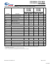
CYDC256B16, CYDC128B16,
CYDC064B16, CYDC128B08,
CYDC064B08
Document #: 001-01638 Rev. *E Page 14 of 26
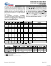
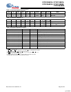
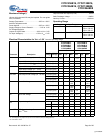
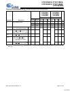
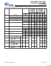
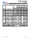
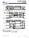
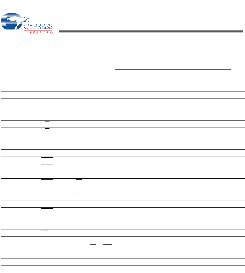
t
HA
Address Hold From Write End 0 0 ns
t
SA
[28]
Address Set-up to Write Start 0 0 ns
t
PWE
Write Pulse Width 25 40 ns
t
SD
Data Set-up to Write End 20 30 ns
t
HD
Data Hold From Write End 0 0 ns
t
HZWE
[30, 31]
R/W LOW to High Z 15 25 ns
t
LZWE
[30, 31]
R/W HIGH to Low Z 0 0 ns
t
WDD
[32]
Write Pulse to Data Delay 55 80 ns
t
DDD
[32]
Write Data Valid to Read Data Valid 55 80 ns
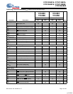
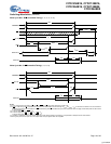
Busy Timing
[33]
t
BLA
BUSY LOW from Address Match 30 45 ns
t
BHA
BUSY HIGH from Address Mismatch 30 45 ns
t
BLC
BUSY LOW from CE LOW 30 45 ns
t
BHC
BUSY HIGH from CE HIGH 30 45 ns
t
PS
[34]
Port Set-up for Priority 5 5 ns
t
WB
R/W HIGH after BUSY (Slave) 0 0 ns
t
WH
R/W HIGH after BUSY HIGH (Slave) 20 35 ns
t
BDD
[35]
BUSY HIGH to Data Valid 30 40 ns
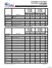
Interrupt Timing
[33]
t
INS
INT Set Time 35 45 ns
t
INR
INT Reset Time 35 45 ns
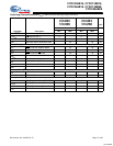
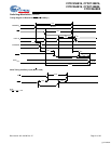
Semaphore Timing
t
SOP
SEM Flag Update Pulse (OE or SEM)10 15 ns
t
SWRD
SEM Flag Write to Read Time 10 10 ns
t
SPS
SEM Flag Contention Window 10 10 ns
t
SAA
SEM Address Access Time 40 55 ns
Notes:
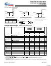
32.For information on port-to-port delay through RAM cells from writing port to reading port, refer to Read Timing with Busy waveform.
33.Test conditions used are Load 2.
34.Add 2ns to this value when the I/O ports are operating at different voltages.
35.t
BDD
is a calculated parameter and is the greater of t
WDD
–t
PWE
(actual) or t
DDD
–t
SD
(actual).
Switching Characteristics for V
CC
= 1.8V Over the Operating Range
[27]
(continued)
Parameter Description
CYDC256B16,
CYDC128B16,
CYDC064B16,
CYDC128B08,
CYDC064B08
CYDC256B16,
CYDC128B16,
CYDC064B16,
CYDC128B08,
CYDC064B08
Unit
-40 -55
Min. Max. Min. Max.
[+] Feedback