


CYDC256B16, CYDC128B16,
CYDC064B16, CYDC128B08,
CYDC064B08
Document #: 001-01638 Rev. *E Page 5 of 26
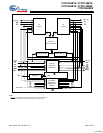
Functional Description
The CYDC256B16, CYDC128B16, CYDC064B16,
CYDC128B08, CYDC064B08 are low-power CMOS 4k,
8k,16k x 16, and 8/16k x 8 dual-port static RAMs. Arbitration
schemes are included on the devices to handle situations
when multiple processors access the same piece of data. Two
ports are provided, permitting independent, asynchronous
access for reads and writes to any location in memory. The
devices can be utilized as standalone 16-bit dual-port static
RAMs or multiple devices can be combined in order to function
as a 32-bit or wider master/slave dual-port static RAM. An M/S
pin is provided for implementing 32-bit or wider memory appli-
cations without the need for separate master and slave
devices or additional discrete logic. Application areas include
interprocessor/multiprocessor designs, communications
status buffering, and dual-port video/graphics memory.
Each port has independent control pins: Chip Enable (CE
),
Read or Write Enable (R/W
), and Output Enable (OE). Two
flags are provided on each port (BUSY
and INT). BUSY
signals that the port is trying to access the same location
currently being accessed by the other port. The Interrupt flag
(INT
) permits communication between ports or systems by
means of a mail box. The semaphores are used to pass a flag,
or token, from one port to the other to indicate that a shared
resource is in use. The semaphore logic is comprised of eight
shared latches. Only one side can control the latch
(semaphore) at any time. Control of a semaphore indicates
that a shared resource is in use. An automatic power-down
feature is controlled independently on each port by a Chip
Enable (CE
) pin.
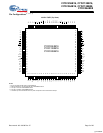
The CYDC256B16, CYDC128B16, CYDC064B16,
CYDC128B08, CYDC064B08 are available in 100-pin TQFP
packages.
Power Supply
The core voltage (V
CC
) can be 1.8V, 2.5V or 3.0V, as long as
it is lower than or equal to the I/O voltage.
Each port can operate on independent I/O voltages. This is
determined by what is connected to the V
DDIOL
and V
DDIOR
pins. The supported I/O standards are 1.8V/2.5V LVCMOS
and 3.0V LVTTL.
Write Operation
Data must be set up for a duration of t
SD
before the rising edge
of R/W
in order to guarantee a valid write. A write operation is
controlled by either the R/W
pin (see Write Cycle No. 1
waveform) or the CE
pin (see Write Cycle No. 2 waveform).
Required inputs for non-contention operations are summa-
rized in Table 1.
If a location is being written to by one port and the opposite
port attempts to read that location, a port-to-port flowthrough
delay must occur before the data is read on the output;
otherwise the data read is not deterministic. Data will be valid
on the port t
DDD
after the data is presented on the other port.
Read Operation
When reading the device, the user must assert both the OE
and CE pins. Data will be available t
ACE
after CE or t
DOE
after
OE
is asserted. If the user wishes to access a semaphore flag,
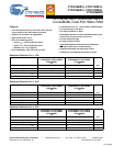
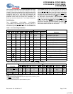
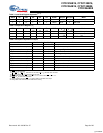
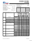
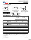
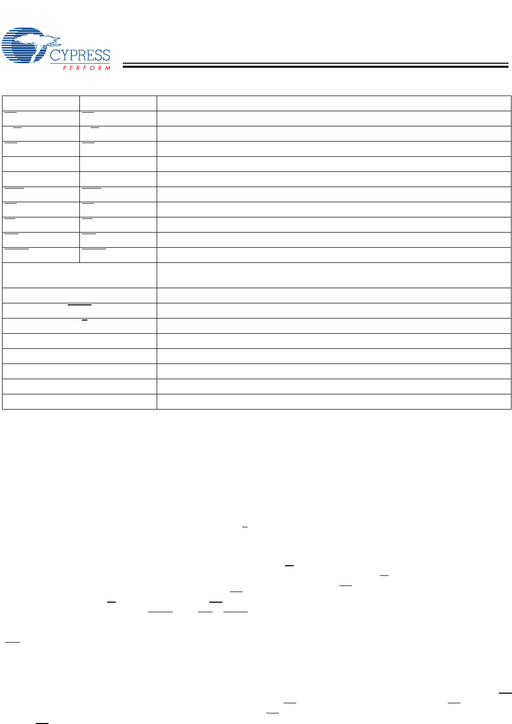
Pin Definitions
Left Port Right Port Description
CE
L
CE
R
Chip Enable
R/W
L
R/W
R
Read/Write Enable
OE
L
OE
R
Output Enable
A
0L
–A
13L
A
0R
–A
13R
Address (A
0
–A
11
for 4k devices; A
0
–A
12
for 8k devices; A
0
–A
13
for 16k devices).
I/O
0L
–I/O
15L
I/O
0R
–I/O
15R
Data Bus Input/Output for x16 devices; I/O
0
–I/O
7
for x8 devices.
SEM
L
SEM
R
Semaphore Enable
UB
L
UB
R
Upper Byte Select (I/O
8
–I/O
15
for x16 devices; Not applicable for x8 devices).
LB
L
LB
R
Lower Byte Select (I/O
0
–I/O
7
for x16 devices; Not applicable for x8 devices).
INT
L
INT
R
Interrupt Flag
BUSY
L
BUSY
R
Busy Flag
IRR0, IRR1 Input Read Register for CYDC064B16, CYDC064B08, CYDC128B16.
A13L, A13R for CYDC256B16 and CYDC128B08 devices.
ODR0-ODR4 Output Drive Register; These outputs are Open Drain.
SFEN
Special Function Enable
M/S
Master or Slave Select
V
CC
Core Power
GND Ground
V
DDIOL
Left Port I/O Voltage
V
DDIOR
Right Port I/O Voltage
NC No Connect. Leave this pin Unconnected.
[+] Feedback